From a distance, the craftwork of prototyping speculative devices is really, really exciting to me. Thinking about design, electronics, construction, developing activated objects that actually work? That’s great.
From 10 millimeters, under a jeweler’s headset with tiny, tiny 30 gauge wires popping off .005 inch integrated circuit pins? I feel like a misunderstood King Kong or something.
I wanted to learn more about debugging at the microscopic scale with hardware, and this seemed as good a time as any. The debugging process essentially takes over the microcontroller, exposing all the little inner secrets — registers, program counters, memory, etc — and lets you step through your code line-by-line. The alternative is either to blink LEDs (if any are attached) and try to assume what might be going on based on that, or the old standard print to output, which means you have to roll a few libraries to actually do that, and have some sort of way of getting the microcontroller’s UART to talk to your computer. (Many of the projects I do have that feature as part of the design, but generally that isn’t always available.)
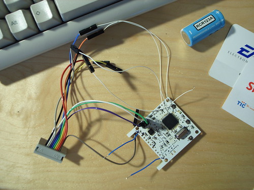
This has been working “okay” for Flavonoid, mostly because I rigged an interface for JTAG boundary scan debugging as an afterthought for this particular spin of the Flavonoid board. You can see it hasn’t gone super great — one of the little 30 gauge white wires there — the one sitting by itself on the right — keeps popping off the MCU, and I’m getting increasingly reluctant to hand solder it back to its pin again. It’s supposed to be attached to one of the multifunction pins on the Atmega324p that’s used for the boundary scan protocol. The heat and possibility of shorts makes me nervous. All the board soldering things on and off causes incremental problems — like the short to ground between a via and the spot on the board where the battery ground attaches just cause a little solder joined them. And the via was to the UART transmit so communication was only one way from the computer to the board, which was perplexing after everything worked. And perplexing for a couple of hours. Hours.
There are craft lessons learned here. Don’t put susceptible vias too close to other things where solder might cause a short, which means more closely inspecting board layout for such things, and creating special rules. Most vias won’t be near something of this sort, but occasionally they will. (Such was the problem with the first run of MobZombies boards where a via was placed way too close to a large ground pad that lived underneath a $35 tiny, leadless gyro.) A book of design rules-of-thumb would be useful to create.
Same with rules about creating accessible debugging test points. I had been conscious of this, but not for the ultra-useful boundary scan debugging. Part of what makes it useful — maybe one of the biggest reasons — is that it exposes all of the registers so you know right away whether you called something by the wrong name by mistake — a common problem when registers are named very similar things and bleary, late-night eyeballs are not as attentive. PORTA PINCA start to look the same after awhile.
There’s also this peculiar boundary scan process that I remember hearing about back in the day what when I was helping design relatively gargantuan integrated circuits. There was this test procedure where you could shift in and out data to individual parts of the device and figure out what was going on inside without having to actually connect directly to the chip. You could essentially send in a message that would set the state of various parts of the chip and retrieve state. There are these bits of logic that essentially sat in between pins and other logic that can either get or set the state of the innards when its in test mode. When your chip isn’t in test mode, the boundary scan cells that sit in there between the pins and logic are made invisible so they don’t effect the operation of the thing. The JTAG part stands for Joint Test Action Group — pretty vague — that was summoned into existence to figure out a standard way for testing digital electronics.
So, well — I think there’s something to be learned here that is not just about the minutiae of electronics and microcontroller debugging. There’s a character of design here that I’m enjoying and that deserves more attention. This is a process that is part of the circulation of ideas — from what is possible to what can be imagined and then, how do you construct it? As I collaborate more and more with innovation groups, designers, products people I am hopeful that more of the craftwork of creating what lies below the surface will be much more integral to the conversations these folks have. So that hardware craftwork is not outsourced but integrated in the concept, design, fabrication process.
Why do I blog this? Thoughts about the process of prototyping/sketching as a kind of design that’s part of “Design.”