A New Logic Analyzer and the HMC6352 I2C Compass

25092008_023841

25092008_024008

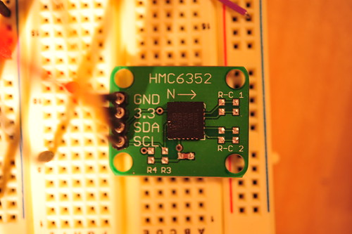
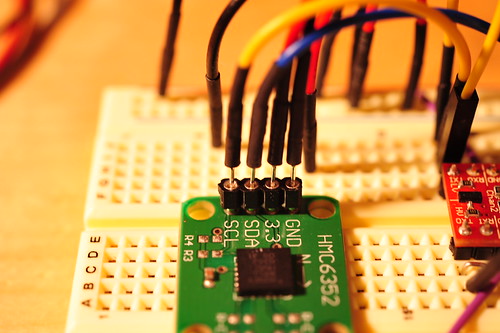
Two things that’ve been sitting on my bench for a good spell — this HMC6352 magnetic compass with an I2C interface, and the Saleae “Logic” logic analyzer. I figured I could combine the two together, showing how I used the Logic to check out the operation of the HMC6352.

First, the HMC6352 is a pretty easy to use magnetic compass with 0.5 degree accuracy. It’s all wrapped up nicely with a pretty normal I2C interface to a bunch of registers on the device, and command-driven queries for reading the compass heading.

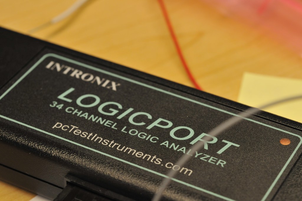
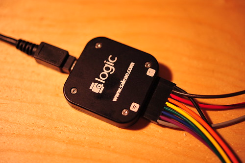
The Saleae “Logic” logic analyzer is pretty sweet for debugging I2C as I’ve mentioned in the past. This one is nice and compact, with a reasonable bunch of logic lines for doing simple analysis. I played with this one for a number of projects over the last few months — mostly I2C projects, which is where most of my interface work is these days. But, the “Logic” will also work with a bunch of stock “analyzers” for RS232 and SPI as well, making it pretty versatile for many situations.

The analyzer is a pretty compact package — 1.6″ square and only .36″ high. So, basically miniature for a logic analyzer. It comes with a 9 conductor umbilical along with E-Z-Hook XKM probes that you can use or not, depending on how you’re hooking up to things.

25092008_024813

25092008_025316

The Logic has a pretty easy-to-use bit of front-end software to handle all the set-up and UI work for the teeny-tiny hardware. It’s a UI that is unlike what you might expect from a bit of Windows-based software. It’s very gooey, using some subtle screen effects and UI elements that, for this OSX guy, are not what I think of when I think of XP. Which is good. It makes using the UI not feel like I’m being forced to drink a Rusty Nail or something for breakfast.

The analyzer samples much quicker than I normally have need for and does so without any problems. I’m usually down in the low range — .2 MHz and 1 M samples is usually plenty for what I’m doing. But, if you need a wider range of samples or a higher sample rate, the analyzer will go all the way up to 24 MHz. Those 9 conductors are 8 data lines plus one ground, so you can analyzer an 8-bit wide bus if you wanted at 24 MHz.

So, I put the Saleae Logic on the HMC6352 circuit to give it a shot. First, the HMC6352 set-up.

Although the HMC6352 has a wide voltage range, I was playing around with a level shifter circuit that was already hooked up to an Arduino on the bench, so I went ahead and just kept that circuit as is. So, the basic set-up is my Arduino I2C lines (SDA and SCL) going through a bi-directional level shifter shifts 3.3V 5V, and then to the HMC6352 SDA and SCL lines. I use yellow wire for SCL and blue wire for SDA.

25092008_024251

25092008_024344

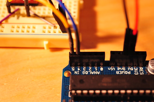
I ended up using the Saleae Logic to dig a bit deeper into the communication between my microcontroller (an Atmega168 sitting on an Arduino) and the HMC6352 as a way to test out the logic analyzer.

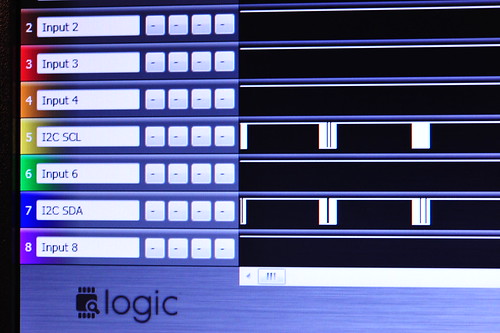
First I wanted to just probe the I2C communication. The basic transaction my Arduino code was doing was to send an “A” to the HMC6352. According to the specification sheet, writing an “A” to the device causes it to return two bytes of data — the high-order and low-order bytes of a 16 bit value indicating the compass’ heading. Easy enough. Here’s the Arduino doing just that. First, it sets up the write to the I2C device at address 0x21. Then it writes an “A” which, in the ASCII table, is the value 0x41. (N.B. The spec sheet says the HMC6352 is at address 0x42 but — and don’t ask me why — sometimes the address specified has to be right-shifted one bit in order to “take”. I mean I sort of know why, but I don’t know why this is the case sometimes — a r/w bit thing or something. Too much to bother with, but a good way to make good use of a logic analyzer when you’re stuck wondering why your device doesn’t seem to be listening to you. I learned this the long way and only had a fancy DSO to try and debug it.)

25092008_025019

25092008_025136

25092008_025615

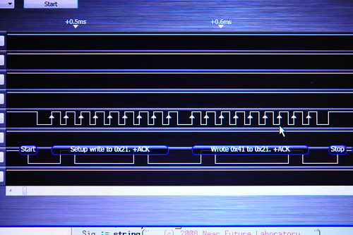
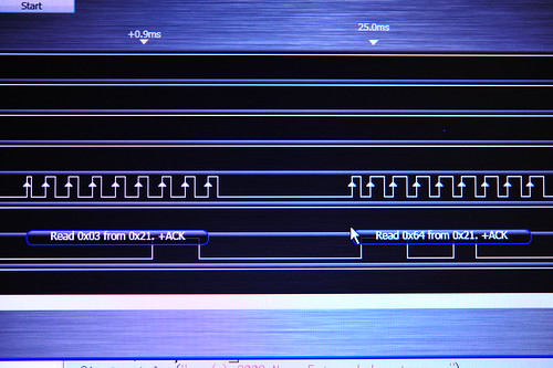
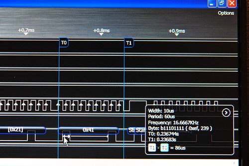
There it is in the top picture. A simple write to the device at address 0x21 with all the ACKs, meaning whatever is out there, heard us and is acknowledging receipt of the write. And, it looks like we get two bytes of data back — a 0x03 and a 0x64. The first byte will be the high-order byte and the second byte is the low-order byte. 0x0364 is 868, which we normalize by dividing by 10, to get 86.8 degrees. Done. I’m pretty sure that’s that. Finally, the measurement features are pretty cool — useful for confirming clock speeds or verifying a bit train. There’s a good use of a simple, pretty inexpensive ($150) logic analyzer that’ll certainly save you $150 worth of your time many times over. Plus, the small size and convenience of USB make it easy enough to fit on your bench and store away or travel around with when it’s not in use. My only quibble is that it’s only for Windows, but that’s a minor one. I don’t really play too hard in the OS religious wars. I run whatever makes my life easier at whatever moment. So, a $200-ish Windows chassis in the laboratory that just runs a few apps like some CAD software and things like my Propeller coding environment, .NET development, software for test equipment like this and AVR Studio 4 — it just helps me get things done rather than being adamantine about which OS religion I’ll adhere to and, then, not getting anything done except spending time porting things from one OS to another or complaining about how much a Windows license costs or whatever.

Wow. Okay. Off my high horse. Check this logic analyzer out. I can recommend it after using it for a few months.

#include

// http://wiring.org.co/reference/libraries/Wire/index.html
// On the Arduino board, Analog In 4 is SDA, Analog In 5 is SCL
// The Wire class handles the TWI transactions, abstracting the nitty-gritty to make
// prototyping easy.
// This sketch has a HMC6352 attached to the I2C bus, through a bi-directional
// level-shifter circuit.
int address = 0x42 >> 1;
 int reading;
void setup()
{

  Serial.begin(9600);

  CLKPR = (1<<clkpce);
  CLKPR = 0;

  // initialize the TWI / I2C Bus
  Wire.begin(); // join i2c bus (address optional for master)

}

void loop() {

  Wire.beginTransmission(address);
  Wire.send('A');
  Wire.endTransmission();
  //delay(10);
  Wire.requestFrom(address, 2);

   if(2 <= Wire.available())    // if two bytes were received
  {
    reading = Wire.receive();  // receive high byte (overwrites previous reading)
    reading = reading << 8;    // shift high byte to be high 8 bits
    reading += Wire.receive(); // receive low byte as lower 8 bits
    reading /= 10;
    Serial.println(reading);   // print the reading
  }

//  delay(50);
}

Continue reading A New Logic Analyzer and the HMC6352 I2C Compass

Logicport Overview

So, just a brief overview here of the Logicport Logic Analyzer and it’s top-line features and set-up. When I set out to figure this thing out, I took a decent “known” set-up that was running a not terribly complicated, but still useful protocol — SPI. As it happens, the Playstation 2 communication between its controller is roughly the SPI protocol, so that’s as good a test as any, seeing as I had been doing some work with the PS2 anyway.

I wrote a bit about that set up already, so this is the part where I describe how I set the Logicport up. Here are links to two other posts related to the Logicport.

PS2 Logic Analysis
Logic Analyzer

There are three main features of the Logicport I’ll describe — Interpreter’s, Triggers and Measurements. (I’ll also briefly describe some of the basic set-up things that I learned.) Interpreters are like templates for specific protocols. The Logicport supports four protocols as these Interpreter “templates — I2C/TWI, SPI, RS232 and CAN 2.0A/2.0B. For the work done at the Near Future Laboratory, we’re basically covered with these.

Creating a new Interpreter from one of these templates is pretty easy. Just with the case of a SPI Interpreter, your job is to specify which of the Logicport’s channels is probing which of the standard SPI channels. In my setup, I configured two different Interpreters — one for the “master” side and one for the “slave” side. On the master side, the Interpreter probes for the MOSI (master-out, slave-in), SCK (serial clock) and SS (slave select — active low) channels. The “slave” side the Interpreter probes for the same stuff, except the data moves across the MISO (master-in, slave-out) channel.

The Interpreter configuration window also allows you to specify a whole bunch of other useful things. First off is the bit order. The PS2 SPI style protocol sends data least-significant bit first, which is okay, but opposite of the canonical SPI protocol. Fortunately, the Interpreter allows you to specify this. You can also tell it how many bits to interpret as data, and what format you want that data to be represented — Hex, Binary, Decimal, Signed or ASCII. So, that’s super useful.

In the lower image above (click it to enlarge it if you need), I’ve set up this additional slave Interpreter, called PSX-MISO-4, to take advantage of a few additional features of the Interpreter. What I wanted to do was isolate the 5th byte of slave data. So, the fifth chunk of information sent by the slave across the MISO channel. In the PS2-controller communication, this represents the right bank of buttons on the controller — triangle, square, circle, ex — as well as the front triggers — L1, L2, R1, R2. (Here’s more information about the frames of data and what they represent.) So, simply for convenience and to make things easy to interpret, I can specify that this particular Interpreter ignore the first 32 bits of data — four bytes — and just start interpreting and showing the data afterwards. Because I _really_ want to isolate this one byte alone, I also tell it to ignore basically everything else after it does the interpretation of the fifth byte — so I just say, ignore the next 800 bits.

[ad#ad-4]

And, you can see in that second image above, that that one byte is represented in binary, which is useful because each of those switches can be interpreted as a 1 (switch open) or a 0 (switch closed or pressed) without converting from decimal or hexadecimal. Here I’m holding down the triangle and ex buttons simultaneously, so bits one and three are 0.

You can also see that the SPI Interpreter allows you to specify the SPI “mode” — clock phase and clock polarity. This can be useful for trying to figure out how an unknown part is actually operating. In my experience, this can be one of the two or three serious “gotchas” when debugging SPI.

Triggers are probably the first thing you’ll set up, but I guess the second thing I’m describing, partially because I haven’t had any complicated triggering scenarios. In the case of the SPI protocol, you want to trigger when the SS line goes low, or active. This is basically saying that the master is beginning to communicate with the slave, which is usually where your interest starts. And this is what this particular Trigger configuration specifies — Trigger when Edge A occurs once. In the main Logicport window, I specify Edge A as a falling signal on the SS line. Easy-peasy. More complicated triggers could be specified, including the variations you can see greyed out in the configuration window. If you had lots of parallel data from a data bus or something you could specify a specific data value, for example. (One thing that would be nice would be to trigger on a specific SPI MOSI value or a specific I2C device address but for reasons I don’t entirely understand, it was explained to me that this is the equivalent of time travel or something. The work-around is to create a debug trigger on an unused signal from your device to indicate that the thing you want to start watching is now happening and use that signal to trigger the Logicport. Fair enough.)

Finally, Measurements. Another very useful and very configurable-y feature. Measurements use either a set of six movable “cursors”, the trigger point or a specific channel to make time-based measurements. You use this Measurement window to specify what you’d like to measure and what you will use to make that measurement. Here I’m using all of them. First, Measurement A is a frequency measurement, using the built-in Hardware Counter (nice..). With this kind of measurement, I have to specify the source, but not in the Measurement Setup window, strangely enough. In the top of the main window, I specify the Measurement A Source as channel D6, which is the blue/white wire from the Logicport. In this case I have clipped that wire to the clock out (CLKO, PB1) of the Atmega324 that’s sitting on my STK500 break-out board. This simply routes the clock signal that the Atmega324 is using to that specific pin. I’ve got a 16MHz crystal connected to the XTAL pins, and so I see a roughly 16,000,000 Hz frequency measurement for Measurement A, as shown in the bottom part of the main window.

Measurement B is a time interval between Cursor A and Cursor B. That’s basically the clock period of the SCK, the SPI clock, which comes out to be 2uS. Measurement C is the same thing, only the frequency of the SPI clock, or 500KHz. Finally Measurement D is the time between Cursor C and Cursor A, which is the time between SS going low and the first bit of MOSI data, 20.1uS. (I could have also specified “Trigger” instead of Cursor C, which might’ve been more accurate.)

These are the main Logicport features I’ve used to get a basic understanding of how it works. It’s pretty straightforward, particularly for simple set ups like this. The other configurations I’ve had to tweak in order to get good analysis has been the sample rate and the logic levels. I’ve had to vary the sample rate, especially when putting a microcontroller on here that’s faster than the sample rate. With the PS2 on its own, and if I’m not measuring signals from a faster microcontroller, I can slow the sample rate down to 1 or 5 MHz. (Not that it matters a whole lot, unless I want to acquire more total samples.) The logic level specifies what counts as logic high (1) and logic low (0) for the logic analyzer. If you specify it too high, your data will go away, or appear flakey, mostly because the logic analyzer is starting to interpret noise or other spurious signals. And, speaking of noise, the Logicport has four wires that are grey wires with black heat shrink. These are for grounding the device to other things, which is crucial to avoid noise. In the case of my setup, I have one grounding the PS2 and another grounding the STK500 breakout board. This creates a common ground across all three boxes and basically eliminates spurious data and other signaling weirdness.