Things That Go To Sleep

Real Time Clock

So, the evolution of machinery has led to the eponymous “sleep” mode, or “sleep state” for digital devices. Our phones and computers and stuff — they can go to sleep. I think the first time I saw this (and was somewhat fascinated) was when a PC I was using had this BIOS that could put the computer into a hibernate mode. The computer could hibernate. It basically powered all the way down, freezing the system state to the hard disk. Like a bear hibernating. Spring time comes and the bear just comes to, presumably — a bit hungry but ready to go. Same with the computer.

So then I start thinking about the bear. And the computer. And the metaphors. Hibernate. Sleep.

They hold up just fine. I mean, it makes sense in a way. Then I start wondering where it goes — in the near future laboratory I’m doing some tinkering to figure out what the near future holds for this metaphor and our digital stuff.

I’ve been tinkering with time quite a bit lately, wondering how it can be used to express or encourage new, hopefully playful interaction rituals for our devices. And I’ve been thinking about a series of devices I’m cobbling together here that are playing in part with time and this is what I want to do.

I want to make devices that go to sleep. I mean, that really do go to sleep. They simply get tired and suspend themselves. Maybe with a bit of a warning like..your laptop battery is running low..I’m going to sleep..even if you change the battery or plug me in..I’m going to sleep, because I’ve been working really hard for the last 3 hours and, well..I’ve just about had it.

Animal Crossing really got me thinking about this in a small, clever, every simple way that every 7 year old understands when they play the game. When our Animal Crossing little hamlet gets dark, people in the game go to sleep. You might come across the occasional night owl, but basically its dark and not a whole lot is going on. And time is coordinated. When it’s nighttime in your normal human world, it is nighttime in your Animal Crossing world. Simple. Makes sense. Games go to sleep. It would be fun to see what life is like if other things do too, imagining that this is one small aspect of the near future we are already starting to inhabit. (Sometimes I wish Twitter would go to sleep.)

Why do I blog this? Shifting the role of the device to that of a more “human” participant is interesting to me — how does this change the terms of interaction? How does it shape the design of things? Do more biologically-derived behaviors shape interaction in playful ways that perhaps lead to more healthful interactions? That reminds us of our own humanity in a way?

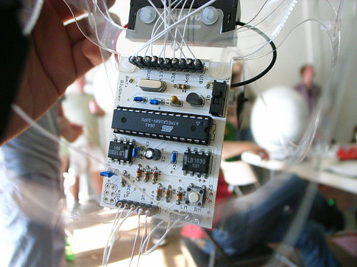
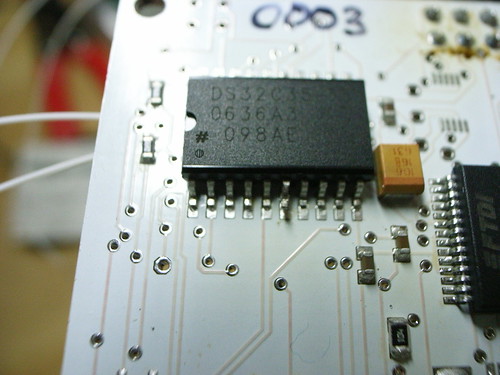
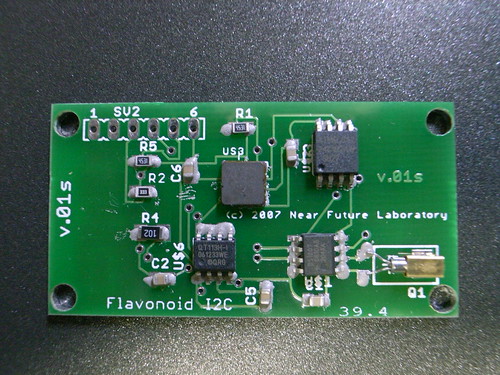
Parenthetically — the chip in that photo? It’s a real-time clock. It’s called the DS32C35 and its made by Maxim IC. It has a couple of alarms built-in that you can set. It knows the time — day, date, month, century, seconds, minutes, hours. It also has a 8kb of FRAM (flash) memory, which is really useful. It replaced the 1 megabit EEPROM I had been using. FRAM is better able to go through very many write cycles whereas EEPROM prefers less (by about an order of magnitude it seems.) Since I’m basically logging data on a frequent basis (recording readings every minute or several minutes), this is a great design alternative. I had also looked at some FRAM devices from Ramtron, but when I found the DS32C35, I integrated it in the design. It also has an on-board crystal, which further reduces the design hassles and parts count. So, when I was using the DS1307, I had to have an external crystal, which took up lots of room, relatively speaking. (You can see it here in the bottom left of this 1st version of Flavonoid.)

Flavonoid v.01s (I2C)

Things That Don't Turn Off

R0014280

Most of the artifacts from the near future I’ve been designing and making have this peculiar property where there’s no on-off switch. I first started thinking about this peculiar idea when I thought about how basically all of my digital stuff just stays on. My laptop. My normal human phone. My mobile phone. These things just stay on all the time. They go to sleep, certainly — but they don’t get switched off entirely.

Why this is interesting? I thought that thinking of our devices and what they do for us as persistent, things we’re always accountable to — in other words, you can’t just cut them off, or silence them or some such thing. More like pet ownership than just having an inert object that can be denied when it is convenient to ignore them, or discard them.

In the near future, our participation with the digitally networked world may be more ambient, with perpetual presence. Our devices will become more like personalities either because of some kind of intelligence (not likely) or because of our human ability to invest personalities in things, even if they don’t have computer chips or dubious “smart appliance” features. These devices will be with us like a good friend or a nagging, poorly trained pet — hide them if you don’t want them around or leave them outside, like a pet — put them in a crib like a baby that needs to rest (and from which you need rest).

Why do I blog this? Making things that don’t turn off forces an entirely new sort of approach to design and functionality that I’m interested in exploring through these designs.

Depth of Field To Add "Depth" To The Interface

PownceFog

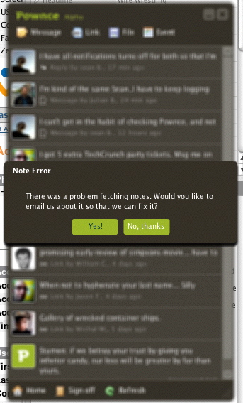
I noticed this while running the little Pownce desktop applet. It moved the window into “the background” by blurring it out a bit as if there were depth to the screen. I’m not 100% sure I like this. I haven’t seen it ever before I don’t think — and it made me wonder if I was getting ready to pass out or something.

I guess I have even more questions about Pownce itself. You know..the service.

area codes

I call Time Warner, the provider of my cable modem line, to troubleshoot the cable modem. I call from my cellphone because I have a VOIP phone that, you know — isn’t working because the cable modem is out of commission. My cellphone has a 917 area code, which is an area code for New York City. Time Warner’s computerized voice telephone answering thing says it can’t help me — I’m calling from New York City. I should hang-up and call another number.

Sigh..

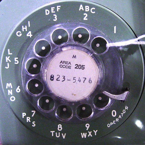
Why do I blog this?It’s curious to me, the relationship between physical geographies and how these have been encoded into digital transactions. It used to be that an telephone area code was very place specific. The areas that were en-coded were often closer to the “real estate” planners determination of a physical place, rather than a municipal determination. In New York City, I can remember advertisements that told you to call “Murray Hill 7-5000”, which translated to rotary dialing MU7-5000. Murray Hill (last I was there) was a peculiar swath east of 5th avenue around 20th up to around 30th or so. There were exchanges like Grand Central, for example, for the area around Grand Central train terminal.

Now of course, area encoding is faulty, but a curious legacy. As soon as telephony went mobile — transportable — it became less specific. With global mobile telephony, its a hold over that I don’t think even is referred to much, except for those who once related to it.

I still find it fascinating. When signing up for GrandCentral‘s new service, I got to pick what area code to assign to my GrandCentral number. Same thing when I got VOIP service — “what geographic place do you want people to identify you with?” — this seems to be the question in that process. Part of the encoding of identity.

Microsoft Research Faculty Summit & Design Expo

Jedi Council Chambers

These are definitely the droids you are looking for..

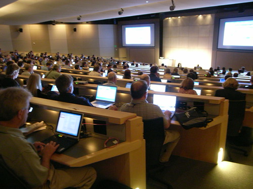
Lili Cheng from Microsoft Research’s Social Computing Group wrangled the student design competitors for MSR’s annual competition. I have to say, this is my bias which shouldn’t be surprising — the design work was much more interesting than the chatter from the Jedi Council about computational thinking stuff. Computational thinking makes me nervous I mean, I understand social groups want to establish that their way of thinking about the world is the way to think about the world, but the epistemological guffaws here are nerve-wracking. I mean, I’m a compute guy, born and raised. I used to snoop around the Princeton University computer lab and all that. But when you start confusing the way you think with the suggestion that that way of thinking describes how every system in the universe operates, you’ve become the little picture in the dictionary next to the definition of hubris. Even the discussion about “interdisciplinary” research or scholarship plainly stated that that meant that computer science would be at the center of the conversation. Like, we’ll write computer programs that will model the computational approaches to, take your pick, economics. And of course we work best with those economist who are inclined to think computationally to begin with, rather than anyone who may think or model in a way that does not fit well within a framework that can be modelled..computationally. I mean..what gives?

Anyway, the saving grace was the design expo and the student design competition. With a close second being the discussions and presentations around the topics of teaching approaches to computer science, even if they were all so computer specific. Sigh..

The competition gave students the challenge to consider health related issues. The student design projects were insightful and playful and had the eagerness of good design ideas (except most did not actually create prototypes beyond screen graphics, a point Bill Moggridge mentioned as criticism on a couple of projects.)

Design Expo

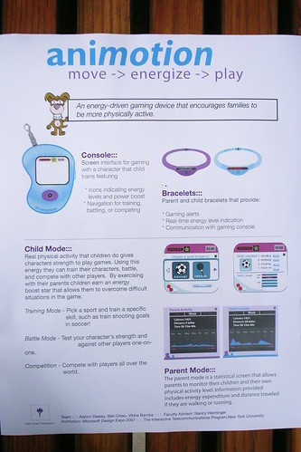
The project that was most intriguing to me was the animotion which is motivated similar to the Flavonoid project. The tagline for animotion goes like this:

An energy-driven gaming device that encourages families to be more physically active.

It consists of a little Console toy, very Tomogotchi-like, that’s a screen interface for gaming with a character that the child trains. And then there are the Bracelets, one for the child and one for the parent. The Bracelets communicate over WiFi (mmmm..) to allow communication with the Console, for real-time energy level indication and for gaming alerts. In Child Mode real physical activity gives characters strength to play games. Move and get power-up. The Parent Mode is a statistical screen that allows parents to monitor their children and their physical activity level. Information provided includes energy expenditure and distance traveled if they are walking or running. I thought this project was interesting obviously because I am working in this area of translating first life activity into second life expressions.

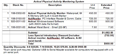
(Usefully, I also learned about this device called Actical which sounds like a data logging three-axis accelerometer. This was some interesting prior art that I had not known about before, so that’s great. It’s a device that can be attached to the hip or ankle or whatever, has a waterproof enclosure and can datalog for days. You then extract the data and do something with it. There are also some studies done to correlate this data to other energy expenditure measures.

ActicalQuote.jpg

The Actical is also way overpriced, or maybe correctly priced for overpriced research studies — I got a quote of $1682 (I’d have to supply my own USB to Serial Adapter). Sheesh. The PC Interface Reader software was $725 — more than the hardware itself, which was $450! Anyway..)

No web page links to the project, but supposedly forthcoming.
(Aislinn Dewey, Ben Chao, Vibha Bamba and Faculty Advisor Nancy Hechinger, ITP NYU)

Design Expo


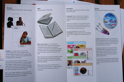
Placematch (in the third column of the brochure above — you can zoom in by clicking the image through to flickr) is a kind of place mat for kids that’s interactive. It has touch-sensivite screens leading the child with the participation of a parent to learn about food and such things through educational activities and short games and animations.ESDI Escola Superior de Desenho Industrialhttp://www.esdi.uerj.br/english

(Alice Geiger, Bernardo Schorr, Bianco Arcadier, Maria Paula Saba)

Design Expo

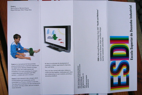
Creat-e is a recreational kit that promotes playing simultaneously in the material and the digital world, allowing children to shape volumes, draw, and create stories and animations. It is a set consisting of e-dough — a digital playdough embedded with RFID sensors — a stylus pen and a receiver.Create-e‘s main element is the e-dough, whose transformations and movements can be transmitted to a TV set or monitor in real time. The stylus pen’s drawings are also transferred to the monitor and may create, add and compose visual elements.Its idea is to simulate the development of creativity in children aged about 6, improving their well-being. They can also connect with other children to create and play together, challenging each other and collaborating on new creations, providing a stimulating feedback.

ESDI Escola Superior de Desenho Industrial
http://www.esdi.uerj.br/english

(Marcio Racca, Mariana Duprat, Miguel Nobrega, Pedro Thiago Silva)

Design Expo

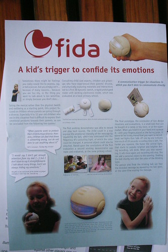
fida

A kid’s trigger to confide its [sic] emotions

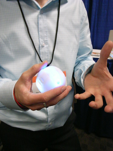
fida is a little org that allows kids to talk to their parents about emotionally challenging things (divorce, etc) that they may be uncomfortable talking about to them directly. So the little org is able to record the child’s voice, and allow them to shake them to show degrees of anger or anxiety. Of course they are illuminated with different colors depending on their state. There devices are articulated so you can squeeze them to open the little clamshell and activate them. They also have these flanges with clips that allow you to add a written note if you want.

Design Expo

This project was interesting because the students constructed a prototype and carefully documented the process and iterations, which I would applaud. They also constructed a prototype that was functional.

It was also curious in the way that it became a kind of note leaving device. As a social practice that’s interesting to me — constructing an asynchronous note that isn’t an instant message similar to Slow Messenger — leaving it behind for someone to find or receive later. The physicality is also quite intriguing — this constructed form and the design + technology work.

More photos of other stuff from the event are here.

Why do I blog this? This was easily the most engaging session of the MSR Faculty Summit. All of the ideas were bright and well-presented. I think there should have been much more emphasis on prior-art. None of the project summarized work that had been done before and how they learned from that earlier work. As Naimark always says on this topic — in the age of Google, there’s really no excuse not to engage and even be in conversation with other people who are shaping the And screen-based designs and concept illustrations are great for evolving the ideas and presenting them, but sketching should include creating some sort of prototype, I believe. It’s part of the design process that should not be excused from concept development.

More PCB Stuff

R0014185

So, I’ve been pretty happy sending printed circuit boards off to this Gold Phoenix operation in China. It feels global to do my manufacturing offshore and its certainly a heck of a lot cheaper than doing it onshore. Frankly, my budget is my pocket money and every penny counts. I’ve been even happier that I can do this stuff all on my own and learn just how these things are made. I mean, it’s one of those things I wish they had maybe taught us back in electrical engineering school, but maybe they thought it was too vocational. Anyway, I really haven’t used a drop of what I learned from back then, honestly. Maybe they taught me how to think or whatever. Who knows.

Anyway, I’ve been overwhelming myself with new projects because I can make my own boards, and being able to have multiple designs fit on one larger panel is really fueling the preposterous number of projects underway. I found out about Gold Phoenix through Nathan/Spark Fun‘s boardhouse batchpcb, which I’ve used in the past. I needed more boards done quicker and in greater quantity than made sense with batchpcb. Nathan never hid the fact that they’re an aggregator for Gold Phoenix, producing amazing prices for very small quantities if you could wait 15 or so days to get them back. For the quantities I needed (couple dozen) it made more sense to go directly to Gold Phoenix.

(You can read this as “Part II” of a review I did earlier of about four board houses.)

So, it’s the same drill to get your boards done, even easier in some regards, but much less hand-holding so you need to pack a reserve ‘chute the first time around. If you have a single design, you basically generate your Gerber‘s the same way you normally do. I even used the Spark Fun Electronics CAM file to generate the Gerber’s. SFE has a tutorial right here for using Eagle to generate Gerber’s. I’ll repeat a few things here.

The Gerber‘s are basically (barely) human readable, but mostly machine readable, text files that describe what goes where on your PCB. For instance, from where to where a bit of copper should go, where a hole goes and how big its diameter. That sort of thing. So, it’s the physical description of your layout, one file for each layer of the board. I’ve only done two layer boards. That is, two layers of copper. Which means that I have six Gerber files plus a drill file. The Gerber’s are one each that describes the top and bottom copper, one each for the top and bottom solder mask, one each for the top and bottom silk screen. Finally, there’s this “NC drill file” used to describe the drilled holes (vias, mounting holes I poke through the board, any through-hole components, etc.) So, that’s six Gerber files and a drill file. You zip those up into a .zip file.

Eagle spits these out when you run the CAM processor using the SFE-Special.cam file that Spark Fun Electronics graciously makes available. It basically does what you need to be done.

Top and bottom silkscreen is a little tricky because it actually pulls the silkscreen from two special layers (_tsilk and _bsilk) that are created by another script (or “ULP” for user library program) also provided by Spark Fun. This other script is called silk_gen.ulp. What it does is make your silk screen drawings a bit “thicker” than the default thickness created by Eagle. It actually copies the geometry and patterns from the normal (by convention) layers that are used to draw paint (silk screened, but I doubt the process involves and actual silk screen nowadays) on the boards. Those layers, best as I can tell, are tPlace and bPlace (top and bottom placement marks for components.) If you run this ULP you’ll see all the tPlace and bPlace redrawn in a different color — and if you check your layers you’ll notice that two more appear in the “Display” pane of Eagle. What happened is that everything in tPlace and bPlace is drawn thicker in _tsilk and _bsilk. You’ll see any text thickened, etc. Evidently, this is necessary for the actual process of applying the silk screen paint to the board.

[ad#ad-4]

The files that you need for production are generated by the CAM Processor. These are:

Top Copper (CMP)
Bottom Copper (SOL)
Top Soldermask (STC)
Bottom Soldermask (STS)
Top Silkscreen (PLC)
Bottom Silkscreen (PLS)
Drill File (DRD)

While we’re talking about layer mishegoss, you’ll notice that there’s also the Dimension layer that looks like it’ll be drawn in paint, but that layer’s geometry does not get drawn as paint — I’m pretty sure it’s used to define the boundaries of the board as the board will be cut out of the panel. I’m not 100% sure how the process works, but empirically — based on runs I’ve done — this’ll allow you to shape the board into whatever shape you need. (See below, some of the boards have slightly rounded edges, and one even has a bit cut out where a battery can fit.) What gets drawn in paint and what doesn’t is determined largely by convention. These “silk” layers are handled by the CAM Processor as layers to be drawn in paint by putting the geometry in the top or bottom silk Gerber files. Whatever geometry you put in that file will get drawn as silk. If you mess up and put your copper geometry in there, they all of your traces and pads and such all will get drawn as paint, which is pretty cool, but something mostly people don’t want. Essentially you’re giving whatever hulking steampunk machine is on the other ed of this instructions on where to lay copper and where to lay paint and where to drill holes and where to cut PCB.

Okay, so — you’re probably better off following Spark Fun’s tutorial, because that’s just a brief summary of the drill you’ll go through. I’m just trying to get to the point of seven Gerber files zipped up into a zip file.

For the Gold Phoenix run, you just email that zip file to their guy Shane in Toronto with a description of what you want. I’ve been taking advantage of these summer specials they’ve been offering. It’s a menu of options such as how big a panel you want your parts cut from? What weight of copper? How thick should the boards be? What color soldermask? What’s your thinnest trace, etc.

For example, for this batch of parts, my order looked like this:

SecondPanel.jpg

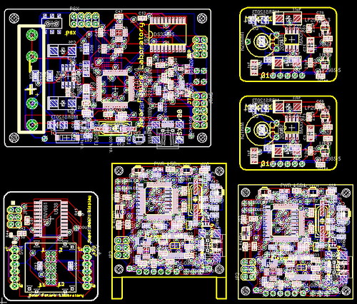
That’s about it. No web form. No drop-down box. My shipping address? I put it in the PayPal form when I paid my $159. I had multiple boards that I put in the layout — those six separate boards? So I had to fork over an extra $30 as a tax for making their lives a little bit harder — fine with me! I get five projects taken care of at once. My board file looked like this (it’s like a board of boards, really):
GoldPhoenix070507.jpg

This was just a board, no schematic. Each one of those individual parts there? They were each designed separately, on their own the usual way. (Create the schematic in Eagle, create a board from the schematic, place parts, route, etc.)

This board of boards was created as a new board design — just a board, not a board and schematic. This is the board design I’ll use to generate Gerbers and drill file for the final thing I send to Gold Phoenix. But, first you need to put all the individual solo-created boards together on this blank board. (I think this is basically what happens when people do what they call panelize or panelizing, but I might be wrong.) You’re basically going to create one board with lots of smaller boards on it. The outlines for each smaller board are what the Gold Phoenix people will use when they cut up the larger board into smaller pieces. They’ll also do the “step and repeat” process of filling up the larger panel with multiple instances of the one board that contains lots of little individual boards.

This is like a three layer Russian Doll. You have your individual boards for some little design projects you’re working on. Then you have this board that contains each of those little board designs, placed thusly so that there’s a little space between them and they don’t overlap and maybe even consume a rectangular shape, etc. Then there’s the “panel” which is the sheet of material that will become a big sold piece of lots of little designs.

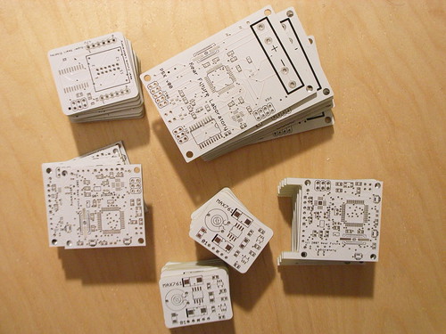
When I got the boards done individually, I turned on all the layers in Eagle, and used Eagle’s “cut” command (confusing..it basically means copy) after selecting everything and placed the individual board on my one larger mothership board. I did that for each design. (One of the designs I put on twice to make the basic outline of the whole thing roughly rectangular. I just sort of assumed that that would make more efficient use of space for the step-and-repeat process of duplicating this design across the larger panel. Todbot thinks that they maybe adjusted the placement of my individual pieces because, by my calculations, I should’ve gotten 9 of each piece and instead I got 10. Anyway, 10 is better than 9.)

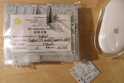
So, what Gold Phoenix ends up doing is taking this one board of boards and making it fit in 1000 square centimeters as many times as they can. This is why I get many copies of each board, 10 in fact of each board because my board of boards can fit 10 times in 1000 square centimeters because its just about 100 cm square (120 actually on my side, but, like Tod said, they must’ve tightened up my board of boards on their end.) They saved me a lot of trouble this way. Rather than me having to make a board of boards 1000 cm square, they do it for me based on my one board of boards template.

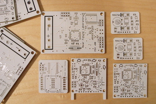
This is what showed up in the FedEx pouch from China 9 Days Later (coulda been sooner if I paid a little extra for extra fast turn-around.)
R0014186

R0014191

I don’t think you can beat that for quality, quantity, time and price with any of the other four or five places I’ve tried. One place was $33 + $40 shipping and handling (scam) for one tiny board, no soldermask (yeech..) no silk, 5 day turn-around. Like..hello?
CfP Special Issue of Convergence: The International Journal of Research Into New Media Technologies

Convergence: The International Journal of Research into New Media Technologies

Call for Papers – Special Issue on ‘Digital Cultures of California
Vol 15 no 1. February 2009

Guest editor:
Julian Bleecker (julian [at] techkwondo [dot] com and bleeckerj [at] gmail [dot] com)
(Near Future Laboratory and University of Southern California)

Please post and circulate

Download Convergence Call for Papers PDF

The deadline for submission of research articles is 1 February 2008.

This call invites submissions for a special issue related to digital cultures of California. Internationally, California is a phenomenon in terms of its relationship to creating, consuming and analyzing the era of digital technologies. From the legendary garage entrepreneurs, to the multi-billion dollar culture of venture capital, to stock back-dating scandals, to the epic exodus of California’s IT support staff during the Burning Man festival, this territory plays an important role in the political, cultural and economic underpinnings of digitally and network-mediated lives on a global scale.

The Bay Area of California (often referred to somewhat incorrectly as Northern California) is perceived as a hot-bed of technology activity. Nearby Silicon Valley serves as a marker for the massive funding of enterprises that shape many aspects of digital culture. The new interaction rituals that have come to define what social life has become in many parts of the world can often be traced back to this part of California. New, popular and curious forms of presence awareness and digital communication such as Twitter and Flickr have found a comfortable home here. Lifestyles of the Northern California digerati have enveloped the cultural milieu, often changing the social landscape to such a degree that it become unrecognizable and unpalatable to those less engaged in creating and consuming digital cultures. Complimenting the Bay Area’s technology production activities is Southern California – the greater Los Angeles basin in particular – where Hollywood sensibilities bring together entertainment with technology through such things as video games, mobile content distribution, digital video and 3D cinema.

California is also the home of several colleges and universities where digital technologies are developed in engineering departments and reflected upon from social science and humanities departments. This curious relationship between production and analysis creates the promise of insightful interdisciplinary approaches to making new kinds of digital networked cultures. Many institutions have made efforts to combine engineering and social science practices to bolster technology design. Xerox PARC probably stands as the canonical example of interdisciplinary approaches to digital technology design. Similarly, combining arts practices with technology as a kind of exploratory research and development has important precedent at places like Intel Berkeley Labs and PARC and at the practice-based events such as the San Jose California-based Zero One festival.

In this special issue we welcome submissions which investigate, provoke and explicate the California digital cultures from a variety of perspectives. We are interested in papers that approach this phenomenon in scholarly and, particularly, approaches that emphasize practice-based analysis and knowledge production.

* What are the ways that social networks have been shaped by digital techniques?

* How has the phenomenon of the digital entrepreneur evolved in the age of DIY sensibilities?

* What are the ways that ‘new ideas’ succeed or fail based on their dissemination amongst the elite, connected digerati, as opposed to their dissemination amongst less more quotidian communities?

* What is the nature of the matrix of relationships between Hollywood entertainment, the military, industry and digital technology?

* Can the DIY culture explored in the pages of Make magazine produce its own markets?

* How does the Apple Inc. culture of product design and development shape and inform popular culture?

* How have the various interdisciplinary approaches undertaken at corporate research centers connected to universities such as Intel Berkeley Labs shaped digital cultures?

* What does ‘Silicon Valley’ mean in other geographies? How has the model of associations between innovation, research and funding been transplanted elsewhere and to what measures of success?

The deadline for submission of research articles is 1 February 2008.

Submissions/proposals for papers should be directed to the guest editor. The special issue will be published (by SAGE) in February 2009. For full details of house style and submission format, please consult www.beds.ac.uk/Convergence

(For all other submissions/inquiries, please contact convergence [at] beds.ac.uk)

Download Convergence Call for Papers PDF

Part 2: Physicality

WiiWhack

The 2nd part of Don Norman’s two part essay on “The Next UI Breakthrough” appears in the July/August 2007 edition of ACM Interactions. In it, he describes how physicality is now being re-introduced into the user interface for computers. He describes physicality as more extensive than tangible computing and “embodiment” (Paul Dourish’s explication of computing that is both social and tangible because the manipulation and handling of objects is always part of social activities.) For Norman, “physicality” is something new in that it is a return after a period of user interfaces in which mechanical manipulation of things like knobs and dials and switches was avoided in favor of things like the so-called soft switches. Now switches and dials have returned, as have more advance interface forms that can respond to gesture.

Physicality: the return to physical devices, where we control things by physical body movement, by turning, moving, and manipulating appropriate mechanical devices.

We have evolved as physical creatures. We live in a complex, three-dimensional world filled with physical objects. We are analog beings in an artificial world of digital devices, devices that abstract what is powerful and good from the physical world and turn it into information spaces, usually in arbitrary ways. These new approaches put the body back into the picture. They require us to control through physical action rather than virtual, which means through mechanical devices, not electronic or graphic.

I’d speculate that part of the return has to do with the fact that the old metaphors of turning a knob, for example, are effective and meaningful. But beyond just switches and control inputs, Norman seems to be speculating that the return to physicality will present opportunities for new kinds of interaction, beyond just switching things on or off, and, hopefully, for interaction beyond typing. Despite Norman’s observation that we’re returning to physical controls, one form of physical control — the keyboard — has never left. I’d be interested in forms of user interface that didn’t even touch the kinds of computing models that keyboards enforce. Can there be a form of computing that relies entirely on physical movement rather than tapping on little plastic squares?

Blimps To Teach

R0013749

R0013759

R0013746

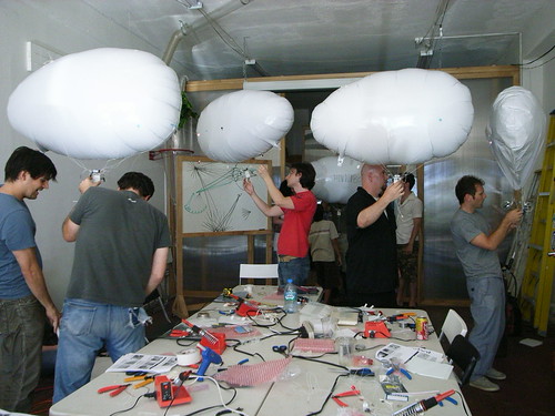
The “Blubber Bot” series of DIY blimps has been a great success. Jed ran a workshop the other day at Machine Project. Sold out, in fact. Everyone was overjoyed. Mark broke out the cooler of ice cream and cones. I think they’re scheduling another one for the people who got locked out.

I’ve been providing Jed with technical and conceptual support for the project and its cousins for a couple of years now. I think this is a great playful interface for learning programming through a simple, fun, interactive toy. Blimps are great fun and placid little house pets. Right now the Blubber Bots have a suite of behaviors that are burned into their microcontroller brain. The next step is to get them closer to the Arduino environment, perhaps. Together with an external library that exposes their various sensors and motors and lights and such all, it would be possible to program your own simple behaviors. Jed’s also talking about a smaller mosquito style blimp with a smaller envelope — maybe the size of a party balloon — with a smaller, surface-mount board for those less inclined to actually do the electronics construction, but perhaps some of the mechanical construction and then writing software for it.

I think that actually constructing something playful, reactive, with personality could go a long way towards teaching art-technology generally, as well as simple principles of microcontrollers, software, playful interface design — all those things. Blinking LEDs are okay, but only go so far in the encouragement department. You have to be prepared to extrapolate blinking LEDs into more playful kinds of interactions and this sort of packs it all into one creature.

Anyway, the Make Magazine people are selling the kit for about $100, which I think is a decent deal. Fun for the whole family and stuff.