Weekending 21012012

Fabien and Nicolas went to Madrid for a workshop at BBVA innovation about Smart Cities. Organized by Urbanscale (and more specifically by Jeff Kirsh, Adam Greenfield and Leah Meisterlin), it focused on opportunities to use networked data for the client. It basically followed up on the previous work we have done with this bank last year.

The workshop went well, with a combination of short talks, field observations (qualitative and quantitative) and discussions. This workshop was followed by an open session entitled “Beyond Smart Cities” at BBVA’s Innovation Center, with Adam Greenfield, myself (Nicolas) and Kevin Slavin. My slides are on Slideshare. There’s a write-up of the event at the following URL. As described by Kevin on his tumblog, “As surely as it feels like a movement has a name (“Smart Cities”) it also feels like the critique of said movement is collectively more articulate and persuasive. Now the key is to find language to describe what it should be, to go beyond popping the balloon and figuring out what the party really needs.“.

Here in Los Angeles Julian has been hard at work puzzling over an incredibly simple problem of making a little audio device called an Ear Freshener avoid having a power switch and a volume knob. He thinks the solution was intimated by a generous comment poster who told him to slap a couple of transistors in strategic locations in the circuit. So he tried that. It seems to make sense. Hopefully it won’t destroy everything.

Related to this were discussions about the principles behind/between things that make sound — such as sound should just come out of them, rather than be all fussy with settings, configurations and network connections. And that tied into an ongoing thinking thing about latter day considerations about “simplicity”, “one thing done well” and skinny Williamsburg/Brick Lane 23 year olds with full beards who’ve done nothing to deserve a full beard but rock Holgas and fetishize film/vinyl/casette tapes fixed-gear bikes and the like. Thus, we’ve been working on a short essay on the topic of the Cult of the Analog Cult. Or something like that.

Meanwhile, on the East side of L.A. Jayne (with Kickstarter funding in hand) has been getting back to making new Portals. They’re still in the physical draft/sketch phase of things but making the upgrade from end-table-foam-core to mdf feels quite satisfying. The insides are still very rough and she’s still getting started with hooking up the magic/technology bits, but at least now a pair of Portal boxes exist in the world, ready to be filled with interactive goodies.

Continue reading Weekending 21012012

LM358 Op-Amp Issues

Audio Mixer Schematic

Should be simple…here’s the test circuit. It’s derived from the multi-channel mixer below. I’m just testing the circuit. It should basically pass through the one input signal perhaps with some attenuation. Instead, it distorts it all to hell-and-gone. Any ideas?

So — back to hammering and less yammering. I’m trying to build a small, portable, DIY audio mixer. Thus far — I’ve found nothing off-the-shelf that meets my, you know..specifications. There are lots of inexpensive and rather expensive field mixers but those are honking things with gigantic XLR inputs for proper microphones. I want about two 1/8″ stereo inputs, and maybe two or three 1/8″ mono inputs. I want to mix a few things and I want the whole thing about the size of deck of cards or something small like that. The only thing I can think to do is to build it.

Plus..we like to build things.

It should be simple but I’m about a decade out of analog electronics. I used to be able to debug op-amp circuits but not any more. And back when I could they didn’t have the internet the way they have now, so I’m sorta putting it out there with as much evidence of the problem as I can muster.

I built the circuit you see above using an LM358 op-amp. Seems like a reasonable go-to unit to build around and many op-amps, as I recall, are generic enough that I feel like it should work in this circuit. (But, I’m prepared to be wrong.)

The problem is that the signal gets super distorted right from the get go.

I’m using my MBP to generate a signal using Max/MSP. It’s just a 1kHz pure tone — a sine wave. The output comes out of the computer, right? Max/MSP generates the signal to go out on one channel and that’s what I feed into my circuit.

Basically — it gets distorted, even at the input. Check out the signal at pin 2 (the + on the left-most op-amp) — it’s what comes after a resistor and capacitor from the input signal. Why’s it so clipped even before it gets processed except for a couple of discrete components? I think that’s the heart of the issue cause the signal doesn’t even touch the op-amp?

So — obviously screen shots from my scope. The top cyan trace is the audio signal I injected into the circuit. It’s a 1kHz sine wave generated from Max/MSP and output over my MacBook’s audio output. It’s about 280mV P-P.

Pin 2 – Basically the input signal after a resistor and capacitor. It’s like..totally clipped there. Why it’s clipped between the raw signal and the input on pin 2 is baffling me. I’ve been so far from analog circuits for so long..I’m just not even sure why putting it on pin 2 alone clips it this way.

The output from the first Op-Amp in the mixer circuit..looks kinda hinky..worse than the input on pin 2.

Things only get worse from there. The output of the first op-amp looks like worse crap. This is basically the op-amp processing one signal and mucking it all up.

Now we’re at pin 6 which is the input to the second op-amp which comes after pin 6 with a 10k resistor in between.

Pin 7 is the final output. This should be a clean signal basically like the input for this test.

Final-final output after a couple of resistors and a capacitor. Distorted crap.

Why do I blog this? Well..I can’t figure out what might be wrong and because the circuit is so simple, I figure the problem is something as simple as the circuit. But, I may be a bit out of my depth and I’m baffled especially because the signal as measured at pin 2 — effectively the input — is distorted already.

Any ideas?

Continue reading LM358 Op-Amp Issues

A Trio Of Posted Things

Friday December 18 16:12

A curious solicitation framework, perhaps done by someone schooled in the layout practices of Ogilvy — attention grabbing image, followed by seductive copy (in French here) and the final *call to action* — Handymen and a phone number. Along the morning bike route, Venice Beach, California.

Thursday December 17 17:08

A desperate plea for a lost week’s pay — and the plea to conscience to do the *right* thing. Seen right here in Venice Beach, California.

Friday December 18 02:29

Finally, the obvious made plain as a reminder. Evidently, it is a fairly common occurrence for distracted self-service pumpers to simply drive off with the pump nozzle still shoved in their tank. These things — I’ve been told — are designed to pop off their couplings without causing a Die Hard style explosion or gasoline fountain. Seen around Calabasas, California.

Continue reading A Trio Of Posted Things

A New Logic Analyzer and the HMC6352 I2C Compass

25092008_023841

25092008_024008

Two things that’ve been sitting on my bench for a good spell — this HMC6352 magnetic compass with an I2C interface, and the Saleae “Logic” logic analyzer. I figured I could combine the two together, showing how I used the Logic to check out the operation of the HMC6352.

First, the HMC6352 is a pretty easy to use magnetic compass with 0.5 degree accuracy. It’s all wrapped up nicely with a pretty normal I2C interface to a bunch of registers on the device, and command-driven queries for reading the compass heading.

The Saleae “Logic” logic analyzer is pretty sweet for debugging I2C as I’ve mentioned in the past. This one is nice and compact, with a reasonable bunch of logic lines for doing simple analysis. I played with this one for a number of projects over the last few months — mostly I2C projects, which is where most of my interface work is these days. But, the “Logic” will also work with a bunch of stock “analyzers” for RS232 and SPI as well, making it pretty versatile for many situations.

The analyzer is a pretty compact package — 1.6″ square and only .36″ high. So, basically miniature for a logic analyzer. It comes with a 9 conductor umbilical along with E-Z-Hook XKM probes that you can use or not, depending on how you’re hooking up to things.

25092008_024813

25092008_025316

The Logic has a pretty easy-to-use bit of front-end software to handle all the set-up and UI work for the teeny-tiny hardware. It’s a UI that is unlike what you might expect from a bit of Windows-based software. It’s very gooey, using some subtle screen effects and UI elements that, for this OSX guy, are not what I think of when I think of XP. Which is good. It makes using the UI not feel like I’m being forced to drink a Rusty Nail or something for breakfast.

The analyzer samples much quicker than I normally have need for and does so without any problems. I’m usually down in the low range — .2 MHz and 1 M samples is usually plenty for what I’m doing. But, if you need a wider range of samples or a higher sample rate, the analyzer will go all the way up to 24 MHz. Those 9 conductors are 8 data lines plus one ground, so you can analyzer an 8-bit wide bus if you wanted at 24 MHz.

So, I put the Saleae Logic on the HMC6352 circuit to give it a shot. First, the HMC6352 set-up.

Although the HMC6352 has a wide voltage range, I was playing around with a level shifter circuit that was already hooked up to an Arduino on the bench, so I went ahead and just kept that circuit as is. So, the basic set-up is my Arduino I2C lines (SDA and SCL) going through a bi-directional level shifter shifts 3.3V 5V, and then to the HMC6352 SDA and SCL lines. I use yellow wire for SCL and blue wire for SDA.

25092008_024251

25092008_024344

I ended up using the Saleae Logic to dig a bit deeper into the communication between my microcontroller (an Atmega168 sitting on an Arduino) and the HMC6352 as a way to test out the logic analyzer.

First I wanted to just probe the I2C communication. The basic transaction my Arduino code was doing was to send an “A” to the HMC6352. According to the specification sheet, writing an “A” to the device causes it to return two bytes of data — the high-order and low-order bytes of a 16 bit value indicating the compass’ heading. Easy enough. Here’s the Arduino doing just that. First, it sets up the write to the I2C device at address 0x21. Then it writes an “A” which, in the ASCII table, is the value 0x41. (N.B. The spec sheet says the HMC6352 is at address 0x42 but — and don’t ask me why — sometimes the address specified has to be right-shifted one bit in order to “take”. I mean I sort of know why, but I don’t know why this is the case sometimes — a r/w bit thing or something. Too much to bother with, but a good way to make good use of a logic analyzer when you’re stuck wondering why your device doesn’t seem to be listening to you. I learned this the long way and only had a fancy DSO to try and debug it.)

25092008_025019

25092008_025136

25092008_025615

There it is in the top picture. A simple write to the device at address 0x21 with all the ACKs, meaning whatever is out there, heard us and is acknowledging receipt of the write. And, it looks like we get two bytes of data back — a 0x03 and a 0x64. The first byte will be the high-order byte and the second byte is the low-order byte. 0x0364 is 868, which we normalize by dividing by 10, to get 86.8 degrees. Done. I’m pretty sure that’s that. Finally, the measurement features are pretty cool — useful for confirming clock speeds or verifying a bit train. There’s a good use of a simple, pretty inexpensive ($150) logic analyzer that’ll certainly save you $150 worth of your time many times over. Plus, the small size and convenience of USB make it easy enough to fit on your bench and store away or travel around with when it’s not in use. My only quibble is that it’s only for Windows, but that’s a minor one. I don’t really play too hard in the OS religious wars. I run whatever makes my life easier at whatever moment. So, a $200-ish Windows chassis in the laboratory that just runs a few apps like some CAD software and things like my Propeller coding environment, .NET development, software for test equipment like this and AVR Studio 4 — it just helps me get things done rather than being adamantine about which OS religion I’ll adhere to and, then, not getting anything done except spending time porting things from one OS to another or complaining about how much a Windows license costs or whatever.

Wow. Okay. Off my high horse. Check this logic analyzer out. I can recommend it after using it for a few months.

#include

// http://wiring.org.co/reference/libraries/Wire/index.html
// On the Arduino board, Analog In 4 is SDA, Analog In 5 is SCL
// The Wire class handles the TWI transactions, abstracting the nitty-gritty to make
// prototyping easy.
// This sketch has a HMC6352 attached to the I2C bus, through a bi-directional
// level-shifter circuit.
int address = 0x42 >> 1;
 int reading;
void setup()
{

  Serial.begin(9600);

  CLKPR = (1<<clkpce);
  CLKPR = 0;

  // initialize the TWI / I2C Bus
  Wire.begin(); // join i2c bus (address optional for master)

}

void loop() {

  Wire.beginTransmission(address);
  Wire.send('A');
  Wire.endTransmission();
  //delay(10);
  Wire.requestFrom(address, 2);

   if(2 <= Wire.available())    // if two bytes were received
  {
    reading = Wire.receive();  // receive high byte (overwrites previous reading)
    reading = reading << 8;    // shift high byte to be high 8 bits
    reading += Wire.receive(); // receive low byte as lower 8 bits
    reading /= 10;
    Serial.println(reading);   // print the reading
  }

//  delay(50);
}

Continue reading A New Logic Analyzer and the HMC6352 I2C Compass

Refining

I’m getting closer to have a second prototype of the PSX project. Strangely, I seem to be building the breadboard prototype (lower image) simultaneous with the PCB prototype (the thing on top). I think the breadboard prototype is mostly for working on the firmware for the Propeller, which is going better than I had hoped, especially seeing as I’ve never developed for it, and that I’m mostly in Spin assembly (not so ugly, but still..bleech..) The breadboard version is basically a core Propeller with some wiring for programming and for chatting to an EEPROM for permanent firmware storage. I started playing with this PCA9306 bidirectional level-shifter, which is sitting on the right half breadboard. This is basically the same circuit as what goes on the surface mount PCB, except for the addition of a LP2985 3.3v regulator.

This is a curious approach, getting slightly ahead of things, but it’s been a circuitous, round-about project from the original “hey..wouldn’t it be cool if..?” motivation that I thought would maybe be a weekend’s work of getting an Atmega324 to emulate a PSX controller. That’s the one in the image above, from last fall. I began the design last summer thinking I’d be done in short order. It should be..I’ve just got grease in my head or something. I was anticipating perhaps some trickiness because I took the trouble to pull out the boundary scan signals to the edge of the board so I could do some JTAG debugging. What went wrong? Well, mostly timing related things. This project motivated me to get my own logic analyzer so I could figure out what the heck was going wrong. There were mostly timing-related problems that I sort of pushed to the side to pursue another possible solution, which led to this current (v07) design.

How did this all start? I thought it’d be an interesting little bit of game controller provocation to have a controller that “got tired” just as one’s avatar might in a video game. To do this, I figured I’d have to Continue reading Refining

Logicport Overview

So, just a brief overview here of the Logicport Logic Analyzer and it’s top-line features and set-up. When I set out to figure this thing out, I took a decent “known” set-up that was running a not terribly complicated, but still useful protocol — SPI. As it happens, the Playstation 2 communication between its controller is roughly the SPI protocol, so that’s as good a test as any, seeing as I had been doing some work with the PS2 anyway.

I wrote a bit about that set up already, so this is the part where I describe how I set the Logicport up. Here are links to two other posts related to the Logicport.

PS2 Logic Analysis
Logic Analyzer

There are three main features of the Logicport I’ll describe — Interpreter’s, Triggers and Measurements. (I’ll also briefly describe some of the basic set-up things that I learned.) Interpreters are like templates for specific protocols. The Logicport supports four protocols as these Interpreter “templates — I2C/TWI, SPI, RS232 and CAN 2.0A/2.0B. For the work done at the Near Future Laboratory, we’re basically covered with these.

Creating a new Interpreter from one of these templates is pretty easy. Just with the case of a SPI Interpreter, your job is to specify which of the Logicport’s channels is probing which of the standard SPI channels. In my setup, I configured two different Interpreters — one for the “master” side and one for the “slave” side. On the master side, the Interpreter probes for the MOSI (master-out, slave-in), SCK (serial clock) and SS (slave select — active low) channels. The “slave” side the Interpreter probes for the same stuff, except the data moves across the MISO (master-in, slave-out) channel.

The Interpreter configuration window also allows you to specify a whole bunch of other useful things. First off is the bit order. The PS2 SPI style protocol sends data least-significant bit first, which is okay, but opposite of the canonical SPI protocol. Fortunately, the Interpreter allows you to specify this. You can also tell it how many bits to interpret as data, and what format you want that data to be represented — Hex, Binary, Decimal, Signed or ASCII. So, that’s super useful.

In the lower image above (click it to enlarge it if you need), I’ve set up this additional slave Interpreter, called PSX-MISO-4, to take advantage of a few additional features of the Interpreter. What I wanted to do was isolate the 5th byte of slave data. So, the fifth chunk of information sent by the slave across the MISO channel. In the PS2-controller communication, this represents the right bank of buttons on the controller — triangle, square, circle, ex — as well as the front triggers — L1, L2, R1, R2. (Here’s more information about the frames of data and what they represent.) So, simply for convenience and to make things easy to interpret, I can specify that this particular Interpreter ignore the first 32 bits of data — four bytes — and just start interpreting and showing the data afterwards. Because I _really_ want to isolate this one byte alone, I also tell it to ignore basically everything else after it does the interpretation of the fifth byte — so I just say, ignore the next 800 bits.

[ad#ad-4]

And, you can see in that second image above, that that one byte is represented in binary, which is useful because each of those switches can be interpreted as a 1 (switch open) or a 0 (switch closed or pressed) without converting from decimal or hexadecimal. Here I’m holding down the triangle and ex buttons simultaneously, so bits one and three are 0.

You can also see that the SPI Interpreter allows you to specify the SPI “mode” — clock phase and clock polarity. This can be useful for trying to figure out how an unknown part is actually operating. In my experience, this can be one of the two or three serious “gotchas” when debugging SPI.

Triggers are probably the first thing you’ll set up, but I guess the second thing I’m describing, partially because I haven’t had any complicated triggering scenarios. In the case of the SPI protocol, you want to trigger when the SS line goes low, or active. This is basically saying that the master is beginning to communicate with the slave, which is usually where your interest starts. And this is what this particular Trigger configuration specifies — Trigger when Edge A occurs once. In the main Logicport window, I specify Edge A as a falling signal on the SS line. Easy-peasy. More complicated triggers could be specified, including the variations you can see greyed out in the configuration window. If you had lots of parallel data from a data bus or something you could specify a specific data value, for example. (One thing that would be nice would be to trigger on a specific SPI MOSI value or a specific I2C device address but for reasons I don’t entirely understand, it was explained to me that this is the equivalent of time travel or something. The work-around is to create a debug trigger on an unused signal from your device to indicate that the thing you want to start watching is now happening and use that signal to trigger the Logicport. Fair enough.)

Finally, Measurements. Another very useful and very configurable-y feature. Measurements use either a set of six movable “cursors”, the trigger point or a specific channel to make time-based measurements. You use this Measurement window to specify what you’d like to measure and what you will use to make that measurement. Here I’m using all of them. First, Measurement A is a frequency measurement, using the built-in Hardware Counter (nice..). With this kind of measurement, I have to specify the source, but not in the Measurement Setup window, strangely enough. In the top of the main window, I specify the Measurement A Source as channel D6, which is the blue/white wire from the Logicport. In this case I have clipped that wire to the clock out (CLKO, PB1) of the Atmega324 that’s sitting on my STK500 break-out board. This simply routes the clock signal that the Atmega324 is using to that specific pin. I’ve got a 16MHz crystal connected to the XTAL pins, and so I see a roughly 16,000,000 Hz frequency measurement for Measurement A, as shown in the bottom part of the main window.

Measurement B is a time interval between Cursor A and Cursor B. That’s basically the clock period of the SCK, the SPI clock, which comes out to be 2uS. Measurement C is the same thing, only the frequency of the SPI clock, or 500KHz. Finally Measurement D is the time between Cursor C and Cursor A, which is the time between SS going low and the first bit of MOSI data, 20.1uS. (I could have also specified “Trigger” instead of Cursor C, which might’ve been more accurate.)

These are the main Logicport features I’ve used to get a basic understanding of how it works. It’s pretty straightforward, particularly for simple set ups like this. The other configurations I’ve had to tweak in order to get good analysis has been the sample rate and the logic levels. I’ve had to vary the sample rate, especially when putting a microcontroller on here that’s faster than the sample rate. With the PS2 on its own, and if I’m not measuring signals from a faster microcontroller, I can slow the sample rate down to 1 or 5 MHz. (Not that it matters a whole lot, unless I want to acquire more total samples.) The logic level specifies what counts as logic high (1) and logic low (0) for the logic analyzer. If you specify it too high, your data will go away, or appear flakey, mostly because the logic analyzer is starting to interpret noise or other spurious signals. And, speaking of noise, the Logicport has four wires that are grey wires with black heat shrink. These are for grounding the device to other things, which is crucial to avoid noise. In the case of my setup, I have one grounding the PS2 and another grounding the STK500 breakout board. This creates a common ground across all three boxes and basically eliminates spurious data and other signaling weirdness.

More PCB Stuff

R0014185

So, I’ve been pretty happy sending printed circuit boards off to this Gold Phoenix operation in China. It feels global to do my manufacturing offshore and its certainly a heck of a lot cheaper than doing it onshore. Frankly, my budget is my pocket money and every penny counts. I’ve been even happier that I can do this stuff all on my own and learn just how these things are made. I mean, it’s one of those things I wish they had maybe taught us back in electrical engineering school, but maybe they thought it was too vocational. Anyway, I really haven’t used a drop of what I learned from back then, honestly. Maybe they taught me how to think or whatever. Who knows.

Anyway, I’ve been overwhelming myself with new projects because I can make my own boards, and being able to have multiple designs fit on one larger panel is really fueling the preposterous number of projects underway. I found out about Gold Phoenix through Nathan/Spark Fun‘s boardhouse batchpcb, which I’ve used in the past. I needed more boards done quicker and in greater quantity than made sense with batchpcb. Nathan never hid the fact that they’re an aggregator for Gold Phoenix, producing amazing prices for very small quantities if you could wait 15 or so days to get them back. For the quantities I needed (couple dozen) it made more sense to go directly to Gold Phoenix.

(You can read this as “Part II” of a review I did earlier of about four board houses.)

So, it’s the same drill to get your boards done, even easier in some regards, but much less hand-holding so you need to pack a reserve ‘chute the first time around. If you have a single design, you basically generate your Gerber‘s the same way you normally do. I even used the Spark Fun Electronics CAM file to generate the Gerber’s. SFE has a tutorial right here for using Eagle to generate Gerber’s. I’ll repeat a few things here.

The Gerber‘s are basically (barely) human readable, but mostly machine readable, text files that describe what goes where on your PCB. For instance, from where to where a bit of copper should go, where a hole goes and how big its diameter. That sort of thing. So, it’s the physical description of your layout, one file for each layer of the board. I’ve only done two layer boards. That is, two layers of copper. Which means that I have six Gerber files plus a drill file. The Gerber’s are one each that describes the top and bottom copper, one each for the top and bottom solder mask, one each for the top and bottom silk screen. Finally, there’s this “NC drill file” used to describe the drilled holes (vias, mounting holes I poke through the board, any through-hole components, etc.) So, that’s six Gerber files and a drill file. You zip those up into a .zip file.

Eagle spits these out when you run the CAM processor using the SFE-Special.cam file that Spark Fun Electronics graciously makes available. It basically does what you need to be done.

Top and bottom silkscreen is a little tricky because it actually pulls the silkscreen from two special layers (_tsilk and _bsilk) that are created by another script (or “ULP” for user library program) also provided by Spark Fun. This other script is called silk_gen.ulp. What it does is make your silk screen drawings a bit “thicker” than the default thickness created by Eagle. It actually copies the geometry and patterns from the normal (by convention) layers that are used to draw paint (silk screened, but I doubt the process involves and actual silk screen nowadays) on the boards. Those layers, best as I can tell, are tPlace and bPlace (top and bottom placement marks for components.) If you run this ULP you’ll see all the tPlace and bPlace redrawn in a different color — and if you check your layers you’ll notice that two more appear in the “Display” pane of Eagle. What happened is that everything in tPlace and bPlace is drawn thicker in _tsilk and _bsilk. You’ll see any text thickened, etc. Evidently, this is necessary for the actual process of applying the silk screen paint to the board.

[ad#ad-4]

The files that you need for production are generated by the CAM Processor. These are:

Top Copper (CMP)
Bottom Copper (SOL)
Top Soldermask (STC)
Bottom Soldermask (STS)
Top Silkscreen (PLC)
Bottom Silkscreen (PLS)
Drill File (DRD)

While we’re talking about layer mishegoss, you’ll notice that there’s also the Dimension layer that looks like it’ll be drawn in paint, but that layer’s geometry does not get drawn as paint — I’m pretty sure it’s used to define the boundaries of the board as the board will be cut out of the panel. I’m not 100% sure how the process works, but empirically — based on runs I’ve done — this’ll allow you to shape the board into whatever shape you need. (See below, some of the boards have slightly rounded edges, and one even has a bit cut out where a battery can fit.) What gets drawn in paint and what doesn’t is determined largely by convention. These “silk” layers are handled by the CAM Processor as layers to be drawn in paint by putting the geometry in the top or bottom silk Gerber files. Whatever geometry you put in that file will get drawn as silk. If you mess up and put your copper geometry in there, they all of your traces and pads and such all will get drawn as paint, which is pretty cool, but something mostly people don’t want. Essentially you’re giving whatever hulking steampunk machine is on the other ed of this instructions on where to lay copper and where to lay paint and where to drill holes and where to cut PCB.

Okay, so — you’re probably better off following Spark Fun’s tutorial, because that’s just a brief summary of the drill you’ll go through. I’m just trying to get to the point of seven Gerber files zipped up into a zip file.

For the Gold Phoenix run, you just email that zip file to their guy Shane in Toronto with a description of what you want. I’ve been taking advantage of these summer specials they’ve been offering. It’s a menu of options such as how big a panel you want your parts cut from? What weight of copper? How thick should the boards be? What color soldermask? What’s your thinnest trace, etc.

For example, for this batch of parts, my order looked like this:

SecondPanel.jpg

That’s about it. No web form. No drop-down box. My shipping address? I put it in the PayPal form when I paid my $159. I had multiple boards that I put in the layout — those six separate boards? So I had to fork over an extra $30 as a tax for making their lives a little bit harder — fine with me! I get five projects taken care of at once. My board file looked like this (it’s like a board of boards, really):

GoldPhoenix070507.jpg

This was just a board, no schematic. Each one of those individual parts there? They were each designed separately, on their own the usual way. (Create the schematic in Eagle, create a board from the schematic, place parts, route, etc.)

This board of boards was created as a new board design — just a board, not a board and schematic. This is the board design I’ll use to generate Gerbers and drill file for the final thing I send to Gold Phoenix. But, first you need to put all the individual solo-created boards together on this blank board. (I think this is basically what happens when people do what they call panelize or panelizing, but I might be wrong.) You’re basically going to create one board with lots of smaller boards on it. The outlines for each smaller board are what the Gold Phoenix people will use when they cut up the larger board into smaller pieces. They’ll also do the “step and repeat” process of filling up the larger panel with multiple instances of the one board that contains lots of little individual boards.

This is like a three layer Russian Doll. You have your individual boards for some little design projects you’re working on. Then you have this board that contains each of those little board designs, placed thusly so that there’s a little space between them and they don’t overlap and maybe even consume a rectangular shape, etc. Then there’s the “panel” which is the sheet of material that will become a big sold piece of lots of little designs.

When I got the boards done individually, I turned on all the layers in Eagle, and used Eagle’s “cut” command (confusing..it basically means copy) after selecting everything and placed the individual board on my one larger mothership board. I did that for each design. (One of the designs I put on twice to make the basic outline of the whole thing roughly rectangular. I just sort of assumed that that would make more efficient use of space for the step-and-repeat process of duplicating this design across the larger panel. Todbot thinks that they maybe adjusted the placement of my individual pieces because, by my calculations, I should’ve gotten 9 of each piece and instead I got 10. Anyway, 10 is better than 9.)

So, what Gold Phoenix ends up doing is taking this one board of boards and making it fit in 1000 square centimeters as many times as they can. This is why I get many copies of each board, 10 in fact of each board because my board of boards can fit 10 times in 1000 square centimeters because its just about 100 cm square (120 actually on my side, but, like Tod said, they must’ve tightened up my board of boards on their end.) They saved me a lot of trouble this way. Rather than me having to make a board of boards 1000 cm square, they do it for me based on my one board of boards template.

This is what showed up in the FedEx pouch from China 9 Days Later (coulda been sooner if I paid a little extra for extra fast turn-around.)

R0014186

R0014191

I don’t think you can beat that for quality, quantity, time and price with any of the other four or five places I’ve tried. One place was $33 + $40 shipping and handling (scam) for one tiny board, no soldermask (yeech..) no silk, 5 day turn-around. Like..hello?

Printed Circuit Board Fab Houses — A Few Reviews

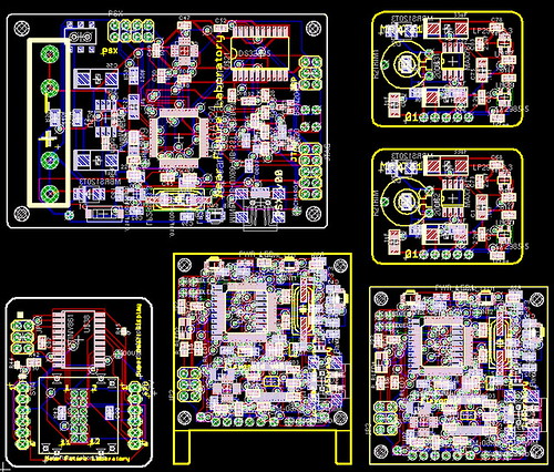
So, I’m at the point with the Flavonoid project that I need to start getting printed circuit boards made. (The printed circuit board includes an accelerometer, a real-time clock, touch sensor, and a bit of EEPROM memory, if you want to know.) A fair bit of the break was spent schooling up on Eagle, doing layouts, making mistakes and that sort of thing. (It’s remarkably full-featured for a free product and, despite a few quirks, does what it says it will do. Plenty of activity in the forums and help is quick to come when I’ve gotten in trouble.)As I closed in on a design I thought was close enough to gold to send off, I started poking around various forums to find out what operation might be suitable for small (1-10 piece) runs.

It turns out that most of the places you’ll hear about won’t do fewer than 5 pieces, and they’ll charge you for it, too. By way of example, I considered trying Advanced Circuits as the Spark Fun FAQ suggests them if you’re in a pinch for time. It’d have to be more than a side-project financed with my own wallet to use them, but maybe they’re better for big projects. (I compare them to the other two board houses near the end of this post.)

The one great exception is Batch PCB, the operation started up by the Spark Fun guys. They’ll do single pieces for, like..$2.50 per square inch. In my limited experience, that’s a great deal. In exchange, you’ll have to wait a bit longer to get your boards back — I think they’ve worked something out with their guy in China so that the numbers work out to get that kind of pricing.

The two places I’m trying are Batch PCB and PCB Fab Express. I picked PCB Fab Express because they had something they refer to as a special for prototypes, but it’s still pretty expensive (but less expensive than other places that’ll turn something around in under a week). I’m doing this so I know what my options are in the future. I can imagine times when waiting a couple of weeks is fine, and other times when I’d like to have something in a few days.

Batch PCB

This is Spark Fun‘s boardhouse operation, which I’d generally just use without even thinking twice, and I have, basically. The one small thing that makes it not necessarily a slam-dunk is the turn-around, which will be at least 10 days. But, that’s probably just fine, except sometimes I feel anxious. But, you know — it’s not like I have customers waiting for product or anything..just me. So, that aside, the Spark Fun guys are friends of the cause and so I support them whenever possible. What you’ll get are 2-layer (seems like they’re doing up to 4 now) boards with pretty much everything. No need to count vias or stuff. Silkscreen on both sides. 8 mil wires and a recommended 10 mils spacing. You can order one board if you want, which is fantastic (as opposed to most other places that make you order 5 of something for which you need only one, or which isn’t 100% yet, so you may end up getting 5 drinks coasters for your $100.) You can put more than one design in your board and just score the two, which can save you some trouble. They have one thing that most places don’t even think to provide — a simple, short-and-sweet Eagle tutorial on preparing your Gerbers. They have a hopped-up forum, where answers to your questions come back pretty lickity-split. Their DRC bot sends you a decent design review summary within a few minutes of uploading your Gerber .zip file (I’m still waiting to get back the DRC from PCB Fab Express, which I sent in a couple of hours ago.)

Flavonoid PCBs from BatchPCB

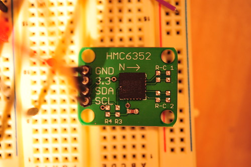
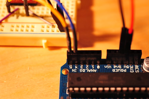
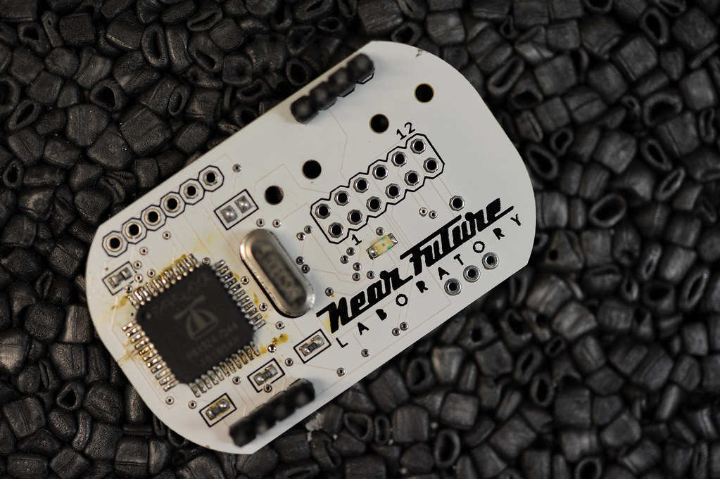
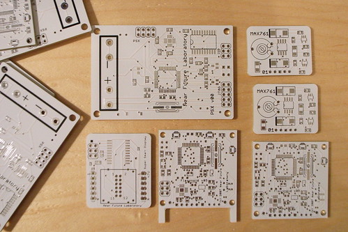
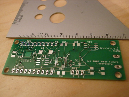
Flavonoid PCB’s just arrived from BatchPCB.com

All-in-all, this is the place to go if you can wait a couple of weeks for your parts. The PCBs you see above were sent in on December 28, and arrived on January 18. Considering generally delays during the holidays, and that Boulder (where those guys are) got socked in by a nasty blizzard, I’d say that’s satisfactory. Total cost for four boards with express shipping was $49.92 Compare to $82.95 for PCB Fab Express, five boards, five days, super-saver shipping. If you’re in a rush or just hopped-up and heads-down in a project, I’d guess the extra $30 is nominal. Note that PCB Fab Express won’t silk screen the back of the board, but that’s not such a big deal in most situations, particularly for prototyping.

One thing I noticed about the boards is that they’re not all 100% the same footprint. By this I mean that the way they were cut out of the larger panel (with probably lots of other people’s boards on it) resulted in slightly different dimensions. I mean, slightly. If you put the boards together like a sticks of gum in a pack, you can tell that some are slightly larger/smaller along the various dimensions. One even seemed slightly curved. This could be an issue if the packaging in which these boards are placed has critical sizing issues. But, it’s ever so slight — nothing that a fine file couldn’t smooth out, if it even caused a problem. (I’m talking about something that’s noticeable if you eyeball it, and measuring, it seems to be about 1mm or less discrepency in size.)

Summary: BatchPCB.com, four boards, silk screen on both sides, 14 business days turn-around, with a blizzard interfering, $49.92 with shipping.

Note that BatchPCB turn-arounds get shorter the more work they do as a company. Presumably, they are able to fill panels sooner and ship whatever minimums they need to their guy in China. Now (January 19) they say they’ll panelize a board in four days, so the turn-around is likely closer to 10 days or thereabouts. That’s fantastic. I also found BatchPCB to be much more “user-friendly”, as is generally the way with the Spark Fun team. (Their tutorials are excellent, particularly the one on does and don’ts for prototyping, all based on real experiences. Don’t forget their surface mount technology tutorials, too, found here. I had two situations where I needed to cancel an order I had submitted. Fortunately, it hadn’t gone too far into the cycle and they could delete the order. Their DRC bot is also quick and provides some useful graphics to give you a sanity check about what precisely you’re submitting.

PCB Fab Express
Okay, this operation seemed a little weird from the get-go, mostly because I got a call about 20 minutes after I created an account. (That sort of bothers me.) But, I talked to the sales guy and was assured that when I submitted by Gerber zip file, I’d get a design review check done and an email back. I submitted my Gerber zip file and must’ve misread something somewhere because my order was put “in process.” The board, my fault completely, had a ground plane copper pour that seemed okay, but I noticed that there were these friggin’ vias going through it. It was just all messed up, but I fixed it in about 3 minutes. Unfortunately, if they even had a DRC, it didn’t catch this (not sure it would’ve, even though it basically meant that nets that shouldn’t connect were connected.)

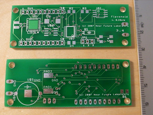
I tried to cancel it (calls and emails) but probably between a mix of my not being as attentive to what I clicked on and the holidays, there was no way to get the order out. I think there’s a problem in the Gerber I sent them, and I’m a bit surprised I didn’t get a DRC email or anything, but..well..I guess chalk that up to experience. (Update — it seems fine after eyeballing the boards I got.) Their prices are a bit more reasonable than other operations for the turn-around — 5 boards, 5 days, $82.95 with tax and “super saver” shipping. They’ll do a finer line spacing than is typical (6 mils). The largest drill hole they’ll do is 246 mils plated, which is fine, only sometimes a mounting hole might be larger, possibly. They have some restrictions on the average number of holes per square inch, which could be annoying if there are lots of vias or whatever. Two-layers, but no silkscreen on the bottom, which one can typically live with for a prototype.The boards just came in, which is exciting. The problem I thought I was going to have didn’t appear for some reason. Unfortunately, I over-wrote the board file from Eagle and so I can’t double-check what I sent them. (I could look at the Gerber’s, though.)

I don’t have all the parts yet, but just a cursory look-see and I thought of a few notes to think about for any redesign.

Flavonoid PCB Prototype Recto

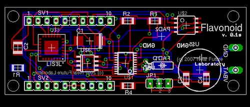
PCB Prototype Recto from PCB Fab Express Flavonoid PCB Prototype Recto

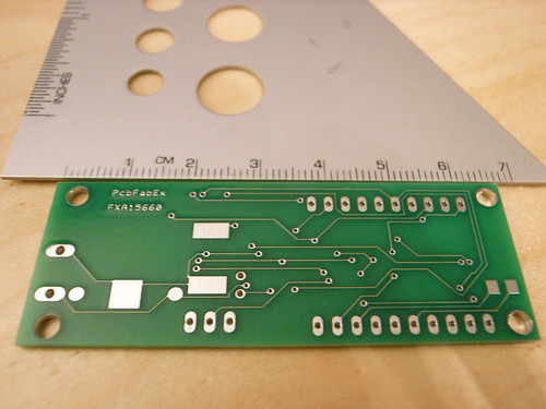
PCB Prototype Verso from PCB Fab Express. Notice there’s no silkscreen on the bottom.* First, some of the vias are unnervingly close to the pins of the DS1306. I’ll look for that in the future and put in a via keepout or something.

* Second, the crystal for the RTC I pulled from the crystal library. The pads for the package aren’t much bigger than a via, and there’s not much of a pad to speak of on the thru-hole. It might be just as well to find an SMT pad for it, or perhaps there’s a package in the crystal library for a surface-mount device.

* The mounting pin for the coin cell battery holder on the back is a bit close to the VBAT pad I put back there. I’m not sure if that mounting pin is connected to anything electrical in the coin cell holder, but I need to check just to be sure.

Summary: Quick turn-around. No hand-holding despite getting a sales call and promise of an email once I submitted. $82.59 with shipping for 5 boards, $16.52 per board, $6.19 per square inch. They took normal Gerber’s RS274X. I used the CAM processor user language program that Spark Fun provides for Eagle in their tutorial.

Advanced Circuits
Expensive and no real reasonable hobbyist pricing for a prototype option. This is probably “okay” for some situations, but certainly not for a hobbyist who’s just looking to get some boards done. No fault, no blame. Just thought I’d add it in since I went through the trouble of checking them out, but I won’t order from them.For comparision, I got a quote from Advanced Circuits for my test case — this Flavonoid PCB that you see above. For a “prototype” run, five boards in 3 days (the longest possible turn-around), it was $47 per board, or $235 without shipping. Their best value deal is 2 days, $57 per board. One day is $61 per board, and same day is $117 per board. Their production pricing — 50 units, say — is $5.86 per board in 2 weeks, or $7.57 a board in 3 days. So, roughly speaking, BatchPCB (described below) is priced in the same ballpark as Advanced Circuits’ production prices, even at single units. My BatchPCB boards came in 2 weeks and cost $7.50 a board ($2.50 per square inch, rounded up.)

Conclusion It’s hard for me to think why I would not use BatchPCB unless I really needed boards quicker than two weeks. If I need something in under a week, I’d go with PCB Fab Express. And, if I really am in some kind of project where I need dozens of printed circuit boards, I’d almost certainly go with BatchPCB — it’s just the best value.

If anyone has any suggestions of other board houses, please drop a line.


R0014191

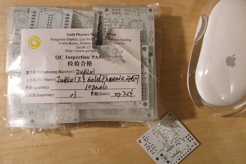
Update! I’ve been using Gold Phoenix when I need more boards as soon as possible — under a week. I haven’t completely run the numbers, but it’s pretty clear that for more than 10 boards or so, they’re the place to go to. If I need just singles of boards and can wait, I’ll use BatchPCB. I have a review of Gold Phoenix here.
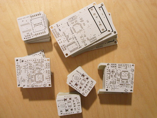
For $89 (special summer deal pricing) you can get 1000 sq centimeters of PCB. When I put six designs on this size, I got 10 of each back. That’s 60 total boards. I paid extra to have some special features like white soldermask and black silkscreen and a $30 tax for multiple designs. Still, it seems like a great deal. Turn-around was under about 12 days.

Arduino and the Two-Wire Interface (TWI/I2C) Including A Short Didactic Parenthetical On Making TWI Work On An Arduino Mini

I have been using the Arduino and Atmel microcontroller’s generally using the SPI (serial-peripheral interface), but decided to look at the two-wire (a.k.a. I2C) interface as well. I’m doing this partially because it would be good to know how it works, but also because it’s electrically more compact. It only uses two-wires, rather than the four required for SPI, so schematic designs and board layouts become a bit more manageable. The trade-off is a little bit more complicated protocols semantics, but nothing out of control. (I’m also looking at using a two-axis accelerometer that’s much less expensive than the three-axis one I’ve been using – $4 versus $15. For some experiments, two-axes may be perfectly fine, and I’m happy to save the $11.)

The first step was making sure the Arduino would handle the TWI – there’s pretty much no reason it shouldn’t, because the Atmega8 certainly handles it. So, the next step was finding out how best to handle TWI transactions.

To do this, I consulted the Atmega8 specification sheet, which has a pretty thorough explanation of the protocol and the implementation details on the Atmega8. (There are also a couple of useful application notes available here and here.) It’s so thorough that I had to print it out. I got a pretty good understanding of how it works but before I started coding, I noticed that there were some TWI libraries both in avrlibc and in the “Wire” library in Wiring.org happens to be packaged as a “sanctioned” external library for Arduino, so that was pretty much that.

Nicholas Zambetti, who wrote the Wire library, pretty much told me it should work with no problems, and he was pretty much right. No problems. His library abstracts the TWI innards really nicely, so I don’t have to muck with any Atmega registers or anything of that sort.

I hooked up my Arduino to a handy accelerometer for testing. (I’m still using the expensive LIS3LV02DQ.) Analog In 4 goes to SDA, and Analog In 5 goes to SCL. I have pull-up resistors on those lines, but Nicolas explains that his library enables the internal pull-ups on the Atmega, so I can probably pull those from my breadboard. Either way, it’s working just fine, even with the external pull-up resistors. (I’m using 4.7k resistors.)

Arduino Mini TWI (I2C)

(I also found in one weird situation that I had to explicitly clear the clock prescaler to get the UART functioning properly. This was while getting TWI working on an AT90USB1287 – TWI worked fine, but the UART was spitting out garbage. On chips where the clock prescaler can be set through the fuses, it’s important to verify that the prescaler isn’t hard wired to divide the clock. This’ll cause anything that is dependent on timing to potentially be off kilter. In my case, the UART was expecting an 8MHz clock to determine timing and baud rate, but the clock was being divided in hardware – not even in the firmware.)

Wire/TWI (I2C) on the Arduino Mini

Getting TWI working on the Arduino Mini (Although the Arduino and Arduino Mini share a name, they don’t share the same processor. The Arduino Mini uses an ATmega168, while the Arduino..normal.. uses an ATmega8. You’ll need to recompile/re-“verify” the Wire library files in order to get TWI to work on the ATmega168/Arduino Mini. There’s a thing or two you’ll have to do by hand to get this to work, and you’ll need to do it each time you move code that’s using the Wire library to a different processor. In other words, when you decide to port the code to the ATmega8, or you put an ATmega16 in your Arduino, or whatever — you’ll need to recompile these libraries. Here’s the drill:

Navigate in a file browser or command prompt to the root of your Arduino file hierarchy. Then go into:

lib/targets/libraries/Wire/
delete Wire.o

lib/targets/libraries/Wire/utility
delete twi.o

Once you’ve done this, make one modification to the header file twi.h in lib/targets/libraries/Wire/utility. Look around line 27 for a commented out line like this:

//#define ATMEGA8

Un-comment it (take out the “//” in the front.) This’ll ensure that the internal pull-up resistors on the ATmega8 are enabled when you’re developing for the normal Arduino. You’ll only need to make this change to twi.h once and for all. Future builds of Arduino should have this fixed.

For those who are curious — pull-up resistors are required on the TWI lines — SCL and SDA. You may use your own external pull-ups, but enabling the internal ones saves you the hassle. But, I don’t think you’ll do much harm if you have the internal one’s enabled and use external ones. But, generally you’ll want to avoid having both internal and external pull-ups.)

Anyway. These modifications described above should get TWI working on the Arduino Mini.)

Here’s the code I wrote and ran:

#include

// TWI (I2C) sketch to communicate with the LIS3LV02DQ accelerometer
// Using the Wire library (created by Nicholas Zambetti)
// http://wiring.org.co/reference/libraries/Wire/index.html
// On the Arduino board, Analog In 4 is SDA, Analog In 5 is SCL
// These correspond to pin 27 (PC4/ADC4/SDA) and pin 28 (PC5/ADC5/SCL) on the Atmega8
// The Wire class handles the TWI transactions, abstracting the nitty-gritty to make
// prototyping easy.

void setup()
{
  pinMode(9, OUTPUT);
  digitalWrite(9, HIGH);
  Serial.begin(9600);

  CLKPR = (1<<clkpce);
  CLKPR = 0;

  Wire.begin(); // join i2c bus (address optional for master)
  Wire.beginTransmission(0x1D);
  Wire.send(0x20); // CTRL_REG1 (20h)
  Wire.send(0x87); // Device on, 40hz, normal mode, all axis's enabled
  Wire.endTransmission();

}

void loop()
{

  byte z_val_l, z_val_h, x_val_l, x_val_h, y_val_l, y_val_h;
  int z_val, x_val, y_val;
  //Serial.println("hello?");
  //byte in_byte;
  // transmit to device with address 0x1D
  // according to the LIS3L* datasheet, the i2c address of is fixed
  // at the factory at 0011101b (0x1D)
  Wire.beginTransmission(0x1D);
  // send the sub address for the register we want to read
  // this is for the OUTZ_H register
  // n.b. supposedly masking the register address with 0x80,
  // you can do multiple reads, with the register address auto-incremented
  Wire.send(0x28);
  // stop transmitting
  Wire.endTransmission();
 // Now do a transfer reading one byte from the LIS3L*
 // This data will be the contents of register 0x28
 Wire.requestFrom(0x1D, 1);
  while(Wire.available())
 {
   x_val_l = Wire.receive();
 }
 Wire.beginTransmission(0x1D); Wire.send(0x29); Wire.endTransmission();
 Wire.requestFrom(0x1D, 1);
 while(Wire.available())
 {
    x_val_h = Wire.receive();
 }
 x_val = x_val_h;
 x_val <<= 8;
 x_val += x_val_l;

 // Y Axis
 Wire.beginTransmission(0x1D); Wire.send(0x2A); Wire.endTransmission();
 Wire.requestFrom(0x1D, 1);
 while(Wire.available())
 {
    y_val_l = Wire.receive();
 }
 Wire.beginTransmission(0x1D); Wire.send(0x2B); Wire.endTransmission();
 Wire.requestFrom(0x1D, 1);
 while(Wire.available())
 {
    y_val_h = Wire.receive();
 }

 y_val = y_val_h;
 y_val <<= 8;
 y_val += y_val_l;

// Z Axis
 Wire.beginTransmission(0x1D); Wire.send(0x2C); Wire.endTransmission();
 Wire.requestFrom(0x1D, 1);
 while(Wire.available())
 {
    z_val_l = Wire.receive();
 }
 Wire.beginTransmission(0x1D); Wire.send(0x2D); Wire.endTransmission();
 Wire.requestFrom(0x1D, 1);
 while(Wire.available())
 {
    z_val_h = Wire.receive();
 }

 z_val = z_val_h;
 z_val <<= 8;
 z_val += z_val_l;
  // Set up to read the next register
  // Supposedly, if you set the most significant bit of
  // the register address to 1, you can do a multiple read,
  // with the register address auto-incrementing. This way, you
  // don't have to do another write — specifying the next register —
  // before reading the next register value. This would be very good, but
  // with a cursory attempt, I have yet to make this work.
/*
    Wire.beginTransmission(0x1D); // transmit to device #4
  Wire.send(0x2C);        // read outx_h
  // stop transmitting
  Wire.endTransmission();
  Wire.requestFrom(0x1D, 1);
 while(Wire.available())
 {
   z_val_l = Wire.receive();
 }

 z_val = z_val_h;
 z_val <<= 8;
 z_val += z_val_l;

  // z axis acceleration, all set.
  // Perfectly still and with the z-axis parallel to the ground, it should be about 1024-ish
  // (I find in practice it is around 1019.)
  // When the z-axis is orthogonal to the ground, it should be zero.
  // 1024 is +1g acceleration, or normal gravity
  // 2048 is +2g
  // 0 is 0g
  Serial.println(z_val, DEC);
*/
Serial.print(x_val, HEX); Serial.print(" ");Serial.print(y_val, HEX); Serial.print(" "); Serial.println(z_val, HEX);
delay(100);
}

Technorati Tags: ,