The Design, Art, Technology & History of Arduino

R0012393

That little guy up above has finally got its own academically written *History. The Arduino is historical! That means something. It means that it is significant enough to warrant a retrospective look back on its when and where and who kinds of questions. I’m glad that’s been done. There are good stories swirling around about Arduino — cafe-bar style stories and anecdotes that you’ll get from the Arduino Wizards like Massimo and Tom and Casey and Golan and Tod. Now Alicia Gibbs has written her masters thesis called New Media Art Design and the Arduino Microcontroller. It’s all about the history and why-for of the Arduino.

The Arduino microcontroller is a malleable tool used in art and design. Started as an educational prototyping tool it contiues to expand due to the thriving community and open source nature. Because open source initiatives allow for modification, derivatives, and sharing of intellectual property, artists and designers can evolve new Arduino-based microcontrollers specified to their work.

Why do I blog this? Alicia sent this to me a couple of months back and I keep trying to find it in my bottomless email database and everytime I do, I forget to blog it so I can have an easy place to find it when I need it. Now — here it is.
Continue reading The Design, Art, Technology & History of Arduino

LIS302DL. A 3 Axis Accelerometer

Tuesday July 14, 13.12.21

Ooooh. Those code jockeys in the Laboratory have been mucking about in the ol’ locker room, giving each other rat-tails, chucking firecrackers in the halls and having a good horsin’ around. Smoking cigarettes and drinking cheap booze. Everything. Stink bombs in the girl’s room. Whatever. It’s a regular Lord of the Flies fest on the electronics wing of the Near Future Laboratory. And, look what we found! Some pole dancin’ hardware porn! Step right up! Don’t crowd..

Wednesday July 15, 13.04.33

In reverent honor of my friends and chums who are holding forth with Sketching in Hardware 09 in London and for the solemn sadness I have for not being able to participate this year, I hereby drop some code and hardware science up on this piece of blog with a dozen or so lines of Arduinoness meant to articulate and instrumentalize the wonderful ST Micro LIS302DL 3 axis accelerometer, delivered here via the Sparkfun breakout board. Without further ado, but with plenty of firmware nakedness, here’s the sketch..*slug* this one’s for you, Sketchers..*sob*

#include

// TWI (I2C) sketch to communicate with the LIS302DL accelerometer
// Using the Wire library (created by Nicholas Zambetti)
// http://wiring.org.co/reference/libraries/Wire/index.html
// On the Arduino board, Analog In 4 is SDA, Analog In 5 is SCL
// These correspond to pin 27 (PC4/ADC4/SDA) and pin 28 (PC5/ADC5/SCL) on the Atmega8 and Atmega168
// The Wire class handles the TWI transactions, abstracting the nitty-gritty to make
// prototyping easy.

// We've got two accelerometers connected. You configure the address of each one
// by some wiring
int address_1 = 0x1C; // SDO on the LIS302DL connected to GND makes it at I2C address 0x1C
int address_2 = 0x1D; // SDO/MISO on the LIS302DL connected to VCC makes it at I2C address 0x1D
void setup()
{
  // we'll use the serial port to spit out our data
  Serial.begin(9600);

  byte tmp;

  Wire.begin(); // join i2c bus (address optional for master)


  // Read from the "WHO_AM_I" register of the LIS302DL and see if it is at
  // the expected address.
  // If it is not, spit out a useful message on the serial port. We'll get
  // erroneous data from querying this address, though.
  Wire.beginTransmission(address_1);
  Wire.send(0x0F);
  Wire.endTransmission();
  Wire.requestFrom(address_1,1);
  while(Wire.available()) {
   tmp = Wire.receive();
   if(tmp != 0x3B) {
     Serial.print("Problem! Can't find device at address "); Serial.println(address_1, HEX);
     delay(1000);
   } else {
  // configure the device's CTRL_REG1 register to initialize it
  Wire.beginTransmission(address_1);
  Wire.send(0x20); // CTRL_REG1 (20h)
  Wire.send(B01000111); // Nominal data rate, Device in active mode, +/- 2g scale, self-tests disabled, all axis's enabled
  Wire.endTransmission();
   }
  }


  // Read from the "WHO_AM_I" register of the second LIS302DL and see if it is at
  // the expected address.
  // If it is not, spit out a useful message on the serial port. We'll get
  // erroneous data from querying this address, though.
  Wire.beginTransmission(address_2);
  Wire.send(0x0F);
  Wire.endTransmission();
  Wire.requestFrom(address_2,1);
  while(Wire.available()) {
   tmp = Wire.receive();
   if(tmp != 0x3B) {
     Serial.print("Problem! Can't find device at address "); Serial.println(address_2, HEX);
     delay(1000);
   } else {

  // configure the device's CTRL_REG1 register to initialize it
  Wire.beginTransmission(address_2);
  Wire.send(0x20); // CTRL_REG1 (20h)
  Wire.send(B01000111); // Nominal data rate, Device in active mode, +/- 2g scale, self-tests disabled, all axis's enabled
  Wire.endTransmission();
   }
  }
}

void loop()
{
  Serial.print("1:"); read_acceleration(address_1);
  Serial.print("2:"); read_acceleration(address_2);
}

void read_acceleration(int address) {
  byte z_val_l, z_val_h, x_val_l, x_val_h, y_val_l, y_val_h;
  int z_val, x_val, y_val;
  Wire.beginTransmission(address);
 // Now do a transfer reading one byte from the LIS302DL
 // This data will be the contents of register 0x29, which is OUT_X
  Wire.send(0x29);
  Wire.endTransmission();
 Wire.requestFrom(address, 1);
  while(Wire.available())
 {
   x_val = Wire.receive();
 }
 // This data will be the contents of register 0x2B which is OUT_Y
 Wire.beginTransmission(address);
 Wire.send(0x2B);
 Wire.endTransmission();
 Wire.requestFrom(address, 1);
 while(Wire.available())
 {
    y_val = Wire.receive();
 }

 // This data will be the contents of register 0x2D, which is OUT_Z
 Wire.beginTransmission(address);
 Wire.send(0x2D);
 Wire.endTransmission();
 Wire.requestFrom(address, 1);
 while(Wire.available())
 {
    z_val = Wire.receive();
 }

 // I want values that run from {-X to 0} and {0 to +X}, so a little bit math goes on here...
 if(bit_is_set(x_val, 7)) {
   x_val &= B01111111;
   x_val = -1*x_val + 128;
   x_val *= -1;
 }

if(bit_is_set(y_val, 7)) {
   y_val &= B01111111;
   y_val = 128 - y_val;
   y_val *= -1;
 }

 if(bit_is_set(z_val, 7)) {
   z_val &= B01111111;
   z_val = 128 - z_val;
   z_val *= -1;
 }

 Serial.print(x_val); Serial.print(":");Serial.print(y_val); Serial.print(":"); Serial.println(z_val);
}

Tuesday July 14, 13.09.59

Wednesday July 15, 14.37.44

What’s going on here? Well, straightforward silliness and hardware gafflin’. Two accelerometers on the I2C bus just cause. It looks like this is as many as you can have on there, unless you do some shenanigans or create a second bus with some cleverness.

The hardware spec on the device (Which. You. Should. Read.) explains that, if we’re going to talk to these things using the I2C bus we need to wire CS to the high end of the logic rail, so VCC. This tells the device that we’ll be using I2C protocol. Then we need to address the device. If we connect the MISO (master in, slave out) pin to GND, then the address will be 0x1C. If we connect the MISO pin to VCC, then the address will be 0x1D. So, MISO, in the I2C configuration, controls the least significant bit of the address. This way, without further mucking about, we can have two accelerometers on the bus, which is probably one more than most situations demand, but just in case.

If I were to connect more than two, I would probably go ahead and use the three-wire protocol and have one microcontroller pin per accelerometer dedicated for chip-select (CS). Fortunately, this device supports three-wire protocols, or the SPI protocol.

Tuesday July 14, 13.17.11

The Arduino code example above does some simple preambling — initializing the two devices after making sure they are there. Then it just loops forever, reading accelerometer data from each of the three axes of each one, doing a little simple bitwise arithmetic to make the data from a negative value for negative g (upside down in most situations) to positive g (right side up, in most situations). The initialization stage sets the accelerometer range — that is, the max/min values it will read — to +/- 2g. (The device will support +/- 8g according to the specifications.)

There are some cool additional features that I don’t play with, including some interrupts that can be triggered if the device falls suddenly, or if it is “clicked/tapped” or “double-clicked/double-tapped”, which is kinda cool, I guess. If you can come up with a non-gratuitous scenario. Which is probably harder than it sounds. But, even in your gratuitous-I-double-click-my-glass-of-Porto-to-signal-the-waiter-I-need-more-Porto the device will save you the hassle of trying to do this sort of interaction semantics in firmware and get you back to finishing what you were doing in the first place.

Why do I blog this? Notes on the integration of hardware to firmware to ideas. This time with a “new” accelerometer that has some pretty neat features. After this, we’ll be going to paper-pulp and line drawings for a bit folks.

Laboratories, Accelerometers And Kitchen Crockery

The Memsic 6202 Accelerometer, fresh out o’the skillet.

We’ve been out of the Laboratory proper — the place where things are constructed and soldered and heated up — for a bit now, not because we don’t go in there, or we haven’t been doing things that will go in there. No, rather, or because of a variety of curiosities that have attracted our attention and, in that way, have slung us around to be more in the mode of reading and observing so as to launch into the next, “next vector of interests.” We believe strongly here allowing things to stew and simmer in the reading-writing-intellect as much as in the making-things section of the young noggin. There is much good that comes from the process of tinkering as well as, err..think-ering, both simultaneously, perhaps. Doing things to help think through what one finds curious or helpful, tinkering our way to new, more habitable world. Making things is a great way to learn. It is also a great way to think-things-through. Rather than the still idle of pondering, as an adjunct to the quiet sit in the cafe — making something that helps add some weight to the thought. Perhaps closer to The Craftsman by Richard Sennett.

The interests today swing around the ways of framing things, explaining and demonstrating and communicating, especially future fictions, perhaps designed fictions, as a way of describing the sometimes peculiar imaginings that get brought upstairs from the boys in the basement in the Bureau of Coming Attractions. We have our Bureau of Urban Scouting, evolving its own practice of observation and, perhaps of more interest, a variety of instruments and procedures for seeing the world sideways. Nicolas and I are in the final stages of this short essay for the Situated Technologies project that will include this topic. Literally in the final stages. As in, right now I should be editing a Google Doc rather than writing this, but I let the morning coffee lead me.

So, this is all to say that this blog swerves constructively, probably baffling all eighteen readers into wondering — what the heck is going on here? Where is the editorial consistency? Where’s my code/diagrams/schematics?

To this I only ask that you look for such things even here, as they are always in-the-making, becoming the hardware in the midst of the thinking-through, in the ideas.

As the curiosity-seeker Jack Schulze recently intoned in a wonderfully Talmudic way"No one cares about what you think, unless you do what you think. No one cares what you do, unless you think about what you do. No one ever really cares what you say."

This may explain Jack’s characteristically quiet demeanor. We’re quite verbally agitated here, so we’ll let the last one slip by us. But, the yammering is the thinking-making-doing, sometimes in words, sometimes in thoughts, sometimes in the materialization of our imagination.

With this said, in response to Reader Number Fourteen’s request this morning for “some code”, I share with you this little thing: Code to Test the Memsic 6202 Accelerometer. You may remember this little guy. We used it in our early foray into fabricating surface-mount electronics. With kitchen skillets. We learned this bit of tinker-y hacker-y from our friends over at Spark Fun. It works great. And it’s cheap as rocks.

I can’t say we were super excited about this particular accelerometer, but that’s okay. It’s just an accelerometer after all. If you follow us down toward the foxhole of these things, you’ll find a whole world of accelerometer fanatics with plenty of material to fuss with — smart accelerometers, accelerometers that let you know when they’re falling, accelerometers that tell you the time as well as whether they’re falling, etc. You’ll find some material buried here in the blog archives, to be exhumed with the right incantation of search and category selection parameters.

This code was written for the Atmel 8-bit microcontrollers that live on the Arduino board. It also makes use of the Wire library for the Arduino, and, as well, the two-wire interface (TWI) hardware support on those microcontrollers, making the whole thing pretty easy-peasy.

#include
#include


// TWI (I2C) sketch to communicate with the Memsic MXC6202J accelerometer
// Using the Wire library (created by Nicholas Zambetti)
// http://wiring.org.co/reference/libraries/Wire/index.html
//
// On the Arduino board, Analog In 4 is SDA, Analog In 5 is SCL
// These correspond to pin 27 (PC4/ADC4/SDA) and pin 28 (PC5/ADC5/SCL) on the Atmega8
// Know You're Microcontroller. Check Which One Is On Your Board/Arduino.
// Newer (as of May '09) Arduinos Use The Atmega168. Can You See It?
// The Wire class handles the TWI transactions, abstracting the nitty-gritty to make
// prototyping easy.

void setup()
{
  Serial.begin(9600);
  Serial.println("Naah??");
  Wire.begin(); // join i2c bus (address optional for master)
}

void loop()
{

  byte x_val_l, x_val_h, y_val_l, y_val_h;
  int x_val, y_val;
// transmit to device with address 0x1D
// according to the MXC6202xMP datasheet, the TWI/I2C address of is fixed
// at the factory depending on what the "x" in the part name is
// Read The Data Sheet section "I2C Bus Data Transfer" for descriptions
// of what the part expects to receive as its address. If you do not understand
// how this works, you are guaranteed to get lost/confusted/frustrated.
// 00010000b is the address of the chip I have, or 0x10

  // a little fuzzy in my recollection here. I think this initializes the chip
  // by setting some bits in the Memsic device's 8-bit internal register
  // Not 100% sure why I initialize two bytes.
  Wire.beginTransmission(0x10);
  Wire.send(0x00);
  Wire.send(0xF0);
  Wire.endTransmission();

  delay(100);

  Wire.beginTransmission(0x10);
  Wire.send(0x00);
  Wire.endTransmission();

  // request five bytes of data
  // first one is the internal register, we can ignore that, but lets look at it for giggles
  Wire.requestFrom(0x10,5);
  while(Wire.available()) {
    Serial.print(Wire.receive(), HEX); // drop the internal register on the floor..
  }
  Serial.println("****");

  // next byte is the MSB of the X axis acceleration
  if(Wire.available()) {
    x_val_h = Wire.receive();
  }
  // next byte is the LSB of the X axis acceleration
  if(Wire.available()) {
    x_val_l = Wire.receive();
  }
  // next byte is the MSB of the Y axis acceleration
  if(Wire.available()) {
    y_val_h = Wire.receive();
  }
  // next byte is the LSB of the Y axis acceleration
  if(Wire.available()) {
    y_val_l = Wire.receive();
  }
  // cobble all of this together into 16 bit acceleration values
  // doing the usual bit-shift polka
  x_val = (x_val_h << 8); x_val |= x_val_l;
  y_val = (y_val_h << 8); y_val |= y_val_l;
  // spit it all out across the serial port so we can see it
  Serial.print(x_val_h, HEX); Serial.print(" "); Serial.print(x_val_l, HEX); Serial.print("n");
  Serial.print(y_val_h, HEX); Serial.print(" "); Serial.print(y_val_l, HEX); Serial.print("n");
  Serial.println("===");

 Wire.endTransmission();

 // loop and do it again.
  delay(200);
}

Continue reading Laboratories, Accelerometers And Kitchen Crockery

Finding The Way – HMC6352 Digital Compass

Friday March 13, 23:53:41

Since I was asked, and asked again, I’ll toss this technotopia solutions nugget to demonstrate that, despite the evidence demonstrated by recent public appearances and weblog postings, we here at the Laboratory are in fact still fully engaged in connecting wires amongst components. Components take a variety of forms, as do the wires. Sometimes bits of silicon strongly encased in hermetically sealed plastic. Other times, cultural components made of different materials. Observations and their conclusions take a variety of paths and sources of inspiration. We enjoy looking at curious people-practices, inspecting them for insights and stories to be told with a variety of resources: objects, images, words.

And so on. More on this point later.

In the meantime, an eager follower has asked for some simple advice that could have been dispatched in an electronic mailing. Instead, The Near Future Laboratory resources room has decided to fold that information into a weblog “posting.”

Wayfinding, of the digital variety has become exceptionally straightforward for those who are okay with writing a dozen or so lines of code for the handy-dandy Arduino and this HMC6352 digital compass which is available as a breakout board off the rack from our friends at Sparkfun.

The compass will give you a perpetual stream of degrees-heading from magnetic north and has interesting adjustments to let you make offset corrections and that sort of thing. It works simply, as all such things should be. It’s a TWI/I2C device, so you get it on the I2C bus, and send commands to its address (42h). Easy-peasy. If you’re doing anything like setting a RAM or EEPROM register, you send the approrpriate command and address. But, for the most part, you’ll just want to tell it to send heading data, right? That’s simple — send the letter ‘A’ (41h) and back comes the heading data. That’s it. Send an ‘A’, get a heading. Send an ‘A’..get a heading. Over and over, or as often as necessary.

Done.

Here’s some Arduino code to get you going!


#include

// http://wiring.org.co/reference/libraries/Wire/index.html
// On the Arduino board, Analog In 4 is SDA, Analog In 5 is SCL
// These correspond to pin 27 (PC4/ADC4/SDA) and pin 28 (PC5/ADC5/SCL) on the Atmega8
//
// These correspond to pin 27 (PC4/SDA/PCINT12/Analog Input 4) and pin 28 (PC5/ADC5/SCL/PCINT13/Analog Input 5) on the Atemga168
// The Wire class handles the TWI transactions, abstracting the nitty-gritty to make
// prototyping easy.

int address = 0x42 >> 1;
 int reading;
void setup()
{
  // this for debugging the data
  Serial.begin(9600);
  // set up
  CLKPR = (1<<clkpce);
  CLKPR = 0;
  // initialize the HMC6352
  Wire.begin(); // join i2c bus (address optional for master)
}

void loop() {

  Wire.beginTransmission(address);
  Wire.send('A');
  Wire.endTransmission();
  //delay(10);
  Wire.requestFrom(address, 2);

   if(2 <= Wire.available())    // if two bytes were received
  {
    reading = Wire.receive();  // receive high byte (overwrites previous reading)
    reading = reading << 8;    // shift high byte to be high 8 bits
    reading += Wire.receive(); // receive low byte as lower 8 bits
    reading /= 10;
    Serial.println(reading);   // print the reading
  }

//  delay(50);
}

Continue reading Finding The Way – HMC6352 Digital Compass

A New Logic Analyzer and the HMC6352 I2C Compass

25092008_023841

25092008_024008

Two things that’ve been sitting on my bench for a good spell — this HMC6352 magnetic compass with an I2C interface, and the Saleae “Logic” logic analyzer. I figured I could combine the two together, showing how I used the Logic to check out the operation of the HMC6352.

First, the HMC6352 is a pretty easy to use magnetic compass with 0.5 degree accuracy. It’s all wrapped up nicely with a pretty normal I2C interface to a bunch of registers on the device, and command-driven queries for reading the compass heading.

The Saleae “Logic” logic analyzer is pretty sweet for debugging I2C as I’ve mentioned in the past. This one is nice and compact, with a reasonable bunch of logic lines for doing simple analysis. I played with this one for a number of projects over the last few months — mostly I2C projects, which is where most of my interface work is these days. But, the “Logic” will also work with a bunch of stock “analyzers” for RS232 and SPI as well, making it pretty versatile for many situations.

The analyzer is a pretty compact package — 1.6″ square and only .36″ high. So, basically miniature for a logic analyzer. It comes with a 9 conductor umbilical along with E-Z-Hook XKM probes that you can use or not, depending on how you’re hooking up to things.

25092008_024813

25092008_025316

The Logic has a pretty easy-to-use bit of front-end software to handle all the set-up and UI work for the teeny-tiny hardware. It’s a UI that is unlike what you might expect from a bit of Windows-based software. It’s very gooey, using some subtle screen effects and UI elements that, for this OSX guy, are not what I think of when I think of XP. Which is good. It makes using the UI not feel like I’m being forced to drink a Rusty Nail or something for breakfast.

The analyzer samples much quicker than I normally have need for and does so without any problems. I’m usually down in the low range — .2 MHz and 1 M samples is usually plenty for what I’m doing. But, if you need a wider range of samples or a higher sample rate, the analyzer will go all the way up to 24 MHz. Those 9 conductors are 8 data lines plus one ground, so you can analyzer an 8-bit wide bus if you wanted at 24 MHz.

So, I put the Saleae Logic on the HMC6352 circuit to give it a shot. First, the HMC6352 set-up.

Although the HMC6352 has a wide voltage range, I was playing around with a level shifter circuit that was already hooked up to an Arduino on the bench, so I went ahead and just kept that circuit as is. So, the basic set-up is my Arduino I2C lines (SDA and SCL) going through a bi-directional level shifter shifts 3.3V 5V, and then to the HMC6352 SDA and SCL lines. I use yellow wire for SCL and blue wire for SDA.

25092008_024251

25092008_024344

I ended up using the Saleae Logic to dig a bit deeper into the communication between my microcontroller (an Atmega168 sitting on an Arduino) and the HMC6352 as a way to test out the logic analyzer.

First I wanted to just probe the I2C communication. The basic transaction my Arduino code was doing was to send an “A” to the HMC6352. According to the specification sheet, writing an “A” to the device causes it to return two bytes of data — the high-order and low-order bytes of a 16 bit value indicating the compass’ heading. Easy enough. Here’s the Arduino doing just that. First, it sets up the write to the I2C device at address 0x21. Then it writes an “A” which, in the ASCII table, is the value 0x41. (N.B. The spec sheet says the HMC6352 is at address 0x42 but — and don’t ask me why — sometimes the address specified has to be right-shifted one bit in order to “take”. I mean I sort of know why, but I don’t know why this is the case sometimes — a r/w bit thing or something. Too much to bother with, but a good way to make good use of a logic analyzer when you’re stuck wondering why your device doesn’t seem to be listening to you. I learned this the long way and only had a fancy DSO to try and debug it.)

25092008_025019

25092008_025136

25092008_025615

There it is in the top picture. A simple write to the device at address 0x21 with all the ACKs, meaning whatever is out there, heard us and is acknowledging receipt of the write. And, it looks like we get two bytes of data back — a 0x03 and a 0x64. The first byte will be the high-order byte and the second byte is the low-order byte. 0x0364 is 868, which we normalize by dividing by 10, to get 86.8 degrees. Done. I’m pretty sure that’s that. Finally, the measurement features are pretty cool — useful for confirming clock speeds or verifying a bit train. There’s a good use of a simple, pretty inexpensive ($150) logic analyzer that’ll certainly save you $150 worth of your time many times over. Plus, the small size and convenience of USB make it easy enough to fit on your bench and store away or travel around with when it’s not in use. My only quibble is that it’s only for Windows, but that’s a minor one. I don’t really play too hard in the OS religious wars. I run whatever makes my life easier at whatever moment. So, a $200-ish Windows chassis in the laboratory that just runs a few apps like some CAD software and things like my Propeller coding environment, .NET development, software for test equipment like this and AVR Studio 4 — it just helps me get things done rather than being adamantine about which OS religion I’ll adhere to and, then, not getting anything done except spending time porting things from one OS to another or complaining about how much a Windows license costs or whatever.

Wow. Okay. Off my high horse. Check this logic analyzer out. I can recommend it after using it for a few months.

#include

// http://wiring.org.co/reference/libraries/Wire/index.html
// On the Arduino board, Analog In 4 is SDA, Analog In 5 is SCL
// The Wire class handles the TWI transactions, abstracting the nitty-gritty to make
// prototyping easy.
// This sketch has a HMC6352 attached to the I2C bus, through a bi-directional
// level-shifter circuit.
int address = 0x42 >> 1;
 int reading;
void setup()
{

  Serial.begin(9600);

  CLKPR = (1<<clkpce);
  CLKPR = 0;

  // initialize the TWI / I2C Bus
  Wire.begin(); // join i2c bus (address optional for master)

}

void loop() {

  Wire.beginTransmission(address);
  Wire.send('A');
  Wire.endTransmission();
  //delay(10);
  Wire.requestFrom(address, 2);

   if(2 <= Wire.available())    // if two bytes were received
  {
    reading = Wire.receive();  // receive high byte (overwrites previous reading)
    reading = reading << 8;    // shift high byte to be high 8 bits
    reading += Wire.receive(); // receive low byte as lower 8 bits
    reading /= 10;
    Serial.println(reading);   // print the reading
  }

//  delay(50);
}

Continue reading A New Logic Analyzer and the HMC6352 I2C Compass

Refining

I’m getting closer to have a second prototype of the PSX project. Strangely, I seem to be building the breadboard prototype (lower image) simultaneous with the PCB prototype (the thing on top). I think the breadboard prototype is mostly for working on the firmware for the Propeller, which is going better than I had hoped, especially seeing as I’ve never developed for it, and that I’m mostly in Spin assembly (not so ugly, but still..bleech..) The breadboard version is basically a core Propeller with some wiring for programming and for chatting to an EEPROM for permanent firmware storage. I started playing with this PCA9306 bidirectional level-shifter, which is sitting on the right half breadboard. This is basically the same circuit as what goes on the surface mount PCB, except for the addition of a LP2985 3.3v regulator.

This is a curious approach, getting slightly ahead of things, but it’s been a circuitous, round-about project from the original “hey..wouldn’t it be cool if..?” motivation that I thought would maybe be a weekend’s work of getting an Atmega324 to emulate a PSX controller. That’s the one in the image above, from last fall. I began the design last summer thinking I’d be done in short order. It should be..I’ve just got grease in my head or something. I was anticipating perhaps some trickiness because I took the trouble to pull out the boundary scan signals to the edge of the board so I could do some JTAG debugging. What went wrong? Well, mostly timing related things. This project motivated me to get my own logic analyzer so I could figure out what the heck was going wrong. There were mostly timing-related problems that I sort of pushed to the side to pursue another possible solution, which led to this current (v07) design.

How did this all start? I thought it’d be an interesting little bit of game controller provocation to have a controller that “got tired” just as one’s avatar might in a video game. To do this, I figured I’d have to Continue reading Refining

PCA9306 Level Shifter

Persistent nagging problem — shifting logic levels between devices that are fabbed with different technologies so their voltages end up being different. Digital circuits “trigger” based on voltage levels — a logic 1 or high signal is relative to the electrical specifications of the device and the fabrication process of the silicon. (A techie diagram is available here.) It’s not a new problem, but one I seem to be coming across more and more as I use the Arduino to do quick sketches of project ideas, or to stand-in for a more embedded solution that might use another of the Atmel 8-bit devices later on when the design and details are more refined.

I’ve tried a bunch of things, including the kind of canonical reference circuit from Philips that uses the BSN20 MOSFET. Sparkfun has a neat little breakout board using a MOSFET, the BSS138. Same principle, built out for you by the fine folk at Sparkfun.

While poking around some more what cause of this PSX project where I have an Arduino trying to talk to a Parallax Propeller, I found reference to a single-chip solution from TI that’s called a PCA9306, which is that small guy up in the photos above. (Just a hair smaller than an 8-pin SSOP package, which means that it was too small to fit on this SSOP break-out — the pins don’t reach the copper, so I had Igor do some hand work to get that to take hold.
Continue reading PCA9306 Level Shifter

PSX..Analog Edition

20080707_02-57-53

So, this is my analog version of a playful Playstation 2 controller for the PSX project — the one that slows the analog part of the controller down over time so, you know..when I’m playing Katamari Damacy it’s a bit more realistic that the Prince gets tired or during GTA, my guy actually gets tired from running away from liquor store heists and stuff.

I’m looking at two approaches. The first is digital — basically intercepting and modifying the communication between the console and the controller. (I’ve described the protocol, and there’s lots of great, hard-gained information out and about describing how it works.)

It’s a good, playful idea as a kind of theory object, entirely doable, kinda complicated and perhaps a bit of an over-designed solution for a simple idea. What I want is something made (constructed, 3D-printed, wired-up, soldered, fab’d, modeled, fussed-over, troubled-with, a cause of grief, etc.) rather than only just discussed. More than discussing only with words (still the greatest instruments for making things) the object also explicates the tension between physical-digital worlds, or the “real world” and “second life”.

This isn’t something that’s a mass-market product design concept, which should be pretty obvious. (Why is it always assumed that productions from the laboratory are products rather than conversation pieces? I would rather make objects that enter into conversations with a provocation, or enter into discussions, raise questions, help create disruptions by describing new interaction rituals, not making least-common denominator products. These are objects that speak — they create, perpetuate and incite discussions — even inspire new concepts that link 1st life with 2nd life, such as “feeding” characters in games in some fashion, which is closer to the motivation than simply trying to hobble a game character. It’s a theory object. The “theory” embodied in the PSX controller concept here is meant to disrupt the conventional understanding of the relationship between physical activity in 1st Life and virtual-physical-digital activity in 2nd Life digital worlds.)

20080707_02-57-20

This is the second, more expeditious design. Basically, I tap right into the PSX controller, putting a microcontroller in between the analog control joysticks and the little FPGA or whatever it is that senses the analog control joysticks. So, my microcontroller determines where the control sticks are and, depending on how long the game’s been played, “dampens” the value, constraining its range.

[ad#ad-4]

It’s a simple “tap” in between, which requires a bit of less-than-elegant de-soldering and pad lifting (or trace cutting) in order to create the cut-in point for the hardware that’ll sense and then spoof the console.

In this case, for testing I used an Arduino, which has enough built-in analog-to-digital converters to sense the positions of the four potentiometers (right-horizontal, right-vertical, left-horizontal, left-vertical) that make up the two joysticks. It also has an I2C/TWI/2-Wire interface that I can use to control four digital potentiometers. The digital potentiometers will appear to be the normal joystick potentiometers only with their values slightly clamped over time to dampen the effects of your normal input.

20080707_04-52-02

The joystick potentiometers produce 8-bit values in the interface protocol, and are around 0x80 (or so..) in the middle, when they haven’t been displaced. Here’s a snip from the larger interface protocol showing, from left to right and in the white trace, right-horizontal, right-vertical, left-horizontal, left-vertical. Each value is in the middle range meaning that the joysticks aren’t displaced. If, for example, the right vertical joystick was fully displaced upward, the second value would be 0x00 (full down would be 0xFF.)

I wrote a simple little Arduino sketch below that does a 10-bit analog-to-digital conversion of the right and left vertical potentiometers. Because the PSX controller seems to have a limited, 8-bit range, it’s necessary to dampen the 10-bit value. Just through experimenting, I found that dividing the 10-bit A2D value by 6 (sort of like right-shifting 2 1/2 times), I could get pretty close to what the controller was producing in terms of a range of values. (I don’t quite get to 0, but it’s close enough.)

I then test attenuating the range by using a constraint function built into the Arduino extended library. This function “clamps” the range of a value passed into it, so I can (in another version) gradually constrain the range that the potentiometer can go through.

Effectively, for this example, when either joystick is full up, the range of the digital potentiometer is clamped, so that the value that the controller senses is not quite a full displacement, no matter how far the player pushes it up. (The same works for downward displacement.) In this case, full upward displacement clamps the right vertical to 0x2B (second from left) and the left vertical to 0x36 (fourth from left). (You can see that the horizontal displacements are off-center because the joystick has been moved and isn’t dead-center in the horizontal direction.)

20080707_04-52-39

20080707_04-47-53

//
// Control the Playstation console
// by spoofing the PSX controller

#include
int RY_Pot = 0;
int LY_Pot = 1;

void setup()
{
  Wire.begin();
  analogReference(EXTERNAL);
  Serial.begin(9600);
}

int val = 0;
int bias = 0;

void loop()
{

  // bias runs between about 23 -90 -  155
 // read the value from the right vertical joystick
  val = analogRead(RY_Pot);

 // transmit to device 0x28
 // which is a DS1803 digital potentiometer
  Wire.beginTransmission(0x28);
// prepare to write to potentiometer-1
  Wire.send(0xAA);
  bias = val/6;
 // Serial.print("RX ");
 // Serial.print(val, DEC);
 // Serial.print(" "); Serial.println(bias, DEC);
 // a bit of fudge..
  if(bias < 30) bias -= 10;
  // sends potentiometer-1 value byte
  Wire.send(constrain(bias+15, 60, 120));
  Wire.endTransmission();

 // do the same thing, for the
 // left vertical joystick
  val = analogRead(LY_Pot);

  Wire.beginTransmission(0x29);
  Wire.send(0xA9);
  bias = val/6;
// Serial.print("RY ");
// Serial.print(val, DEC);
// Serial.print(" ");
// Serial.println(bias, DEC);
  if(bias < 30) bias -= 10;
 // sends potentiometer value byte
  Wire.send(constrain(bias+15, 60, 120));
  Wire.endTransmission();     // stop transmitting

  //delay(100);
}

DS1803 Digital Potentiometer

I’ve been fussing with this digital potentiometer, the DS1803 by Maxim. They’re “digital” because you can control the resistance over its range programmatically, by sending it commands over a 2-Wire (I2C/TWI) serial interface. So, that means that I can hook it up to some microcontroller, like the Arduino, and adjust the resistance in a little program. I chose this one in particular because it can operate at either 3V or 5V, which is convenient, and it comes in a few different models with various resistance ranges. I’m using the DS1803-010, which means it has a range of 0-10K Ohms.

I created a little PCB with two DS1803s on it. Each DS1803 has two potentiometers on it, so I’ve got four on this board. The code for controlling the DS1803 is pretty straightforward. Each one is addressable over the 2-Wire interface, but because we have two on the same interface, I had to configure one to listen to a slightly different address. The details are in the specification sheet, but basically you hardwire the three lines A0, A1, A2 (see the schematic above) to change the address. Effectively you can have up to 8 individually addressable DS1803s on one interface.

In the Arduino source code example below I am only talking with one DS1803 at address 0x28. (if I was talking to to the second one in the schematic, its address was 0x29.) Here I’ve hooked up a logic analyzer to the interface to just make sure we’re communicating. The code below simply adjusts the potentiometer incrementally upward.

[ad#ad-4]

//
// Control the DS1803 Digital Potentiometer

#include <Wire.h>

void setup()
{
  Wire.begin(); // join i2c bus (address optional for master)
}

byte val = 0;

void loop()
{
  Wire.beginTransmission(0x28); // transmit to device 0x28)
  Wire.send(0xAA);            // sends instruction byte,
                               // write to potentiometer-0
  Wire.send(val);             // sends potentiometer value byte
  Wire.endTransmission();     // stop transmitting

  val++;        // increment value
  if(val == 150) // if reached 64th position (max)
  {
    val = 0;    // start over from lowest value
  }
  delay(100);
}


I2C Logic Analysis

20080527_17-42-21

I’ve been doing a bit of business trying to clean up my sometimes wonky skills with I2C communication. It took a bit to figure it out, but I managed to get a few different kinds of devices to the Atmel microcontrollers I usually use — things like a real-time clock, an LIS3LV02DQ accelerometer, these EEPROM devices. Often enough, the first time I connect something new, I confuse some part of the protocol.

Being someone who prefers to see what’s going on rather than poke around and check for what might be a loose connection somewhere, I finally decided to get a logic analyzer. That way, I could take a bit of guesswork out of what was (not) going on. (Sometimes I’ve used my digital oscilloscope, which does the trick too for tracing signals, but then you have to do a bunch of counting bits on the scope — I get confused with such things, especially late at night.)

There are two other posts about this Logicport device, which you may be interested in.

Logicport Overview
PS2 Logic Analysis

(Click the image to try out Cabel Maxfield Sasser’s FancyZoom thingie, pluginifized by Stephen Granade. A new Near Future Laboratory feature!)

20080527_17-39-51

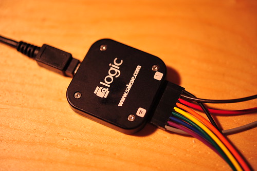
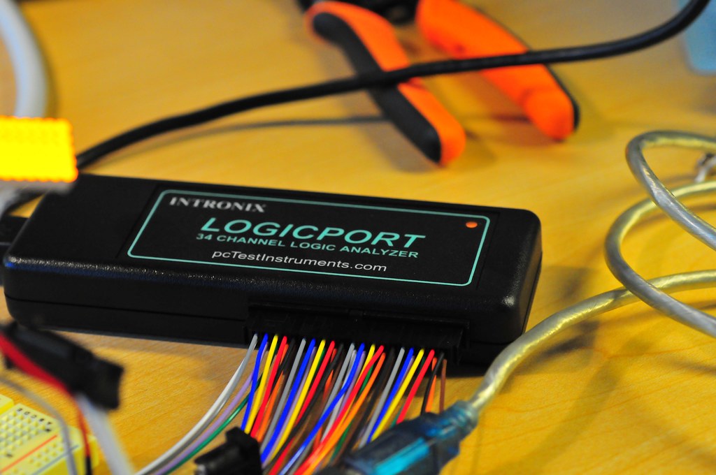
I recently got a hold of one of these Logicport devices from Intronix. It costs $384, and I got a bunch of these nifty “XKM” grabber hook things which are pretty essentially for fastening to small leads or the ends of wires. It’s got 34 channels that it can sample at 500MHz (200MHz if using an external clock..not 100% sure why its slower with an external clock, but okay..), plus built in “interpreters” for some protocols I’m bound to come across, like I2C, SPI, CAN and RS232. The instrument itself connects to your PC (a “PC” PC, not any old personal computer) where the GUI runs. So, unlike a mega-expensive benchtop logic analyzer, you can use a somewhat junker PC and have a decent logic analysis set up for less than $1000. (Or, run Parallels on your Mac and do it there — seems to work just fine.)

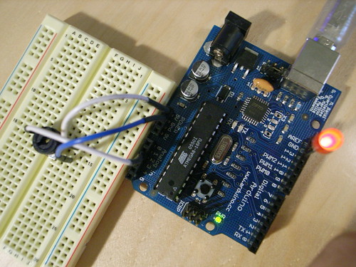
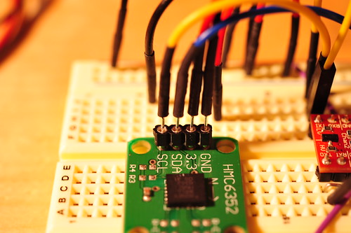
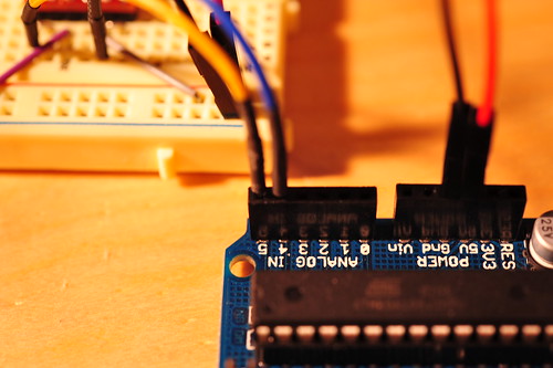
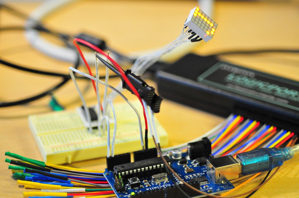
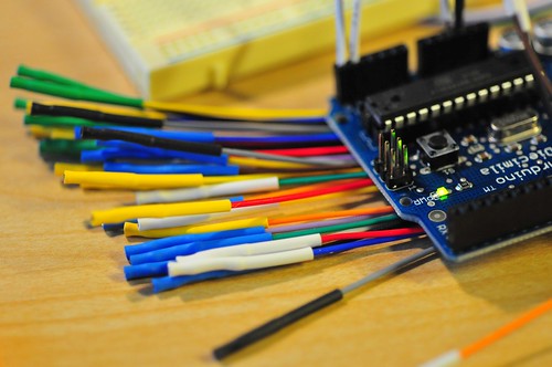
Here’s an Arduino that’s being used to control a MAX6953. The connection to the Arduino and the Logicport is pretty straightforward. Basically, I run an additional wire in parallel to Arduino analog in 4 and 5 which are the I2C lines SDA and SCL respectively. But, you could connect directly to the Atmega168 pins 28 and 27 right there on the chip just as easily if you’re using those useful XKM grabber things.

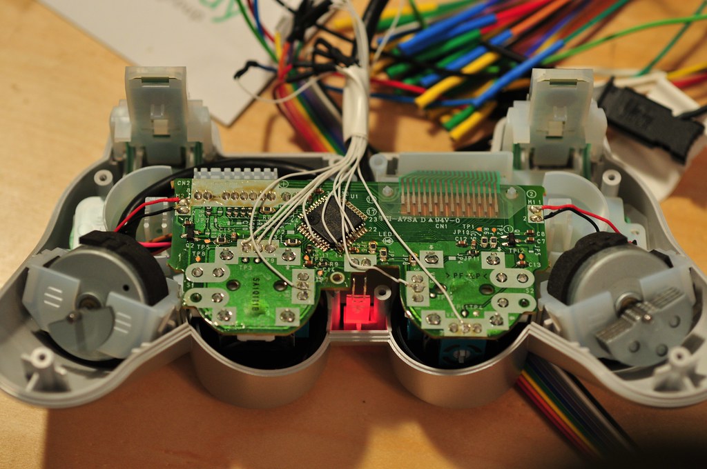
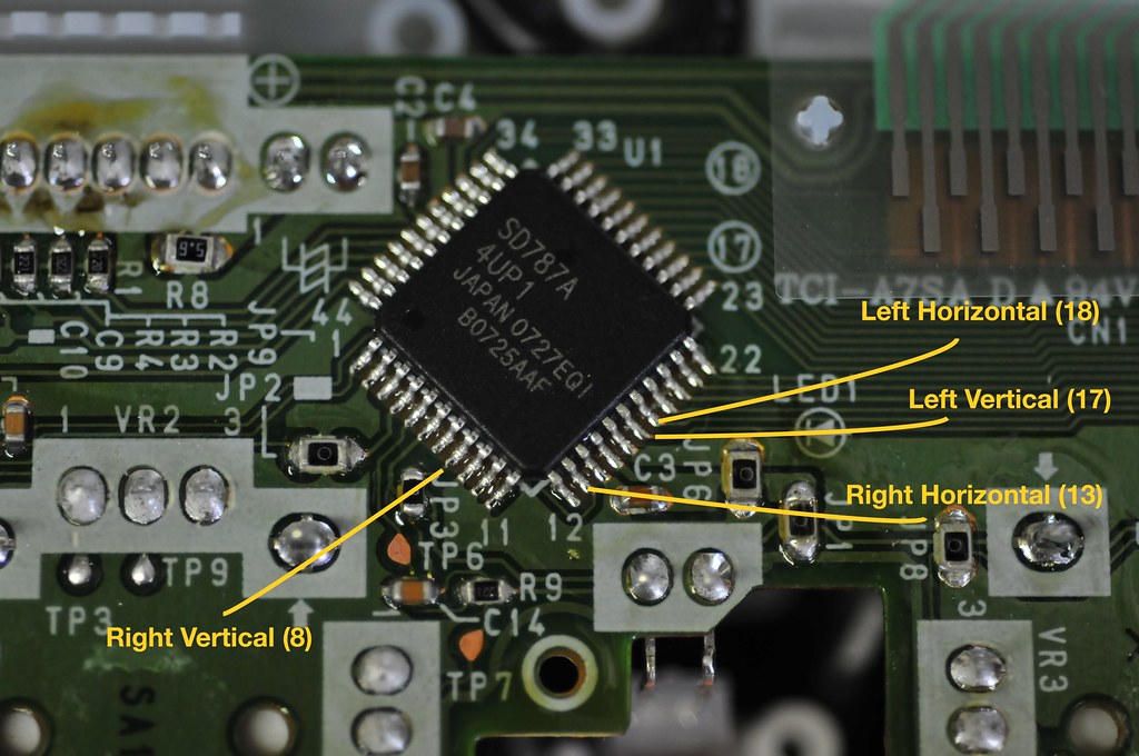
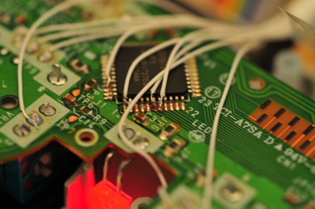
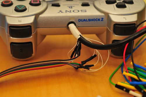
I mostly got this thing because I end up doing lots of I2C connected device kinda projects, where I’ll have some microcontroller like a PIC or Atmega communicating with some I2C digital potentiometer or display driver, etc. (Ultimately though I was _really_ motivated to get it while trying to get my Playstation 2 to allow itself to be controlled by an Atmega. It should work in theory, but there may be some timing related issues that were proving intractable to debug with just a normal oscilloscope. Hopefully this thing will help.)

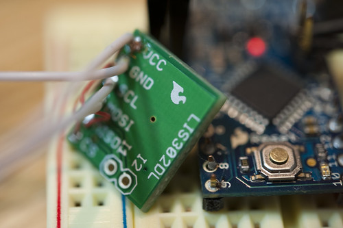
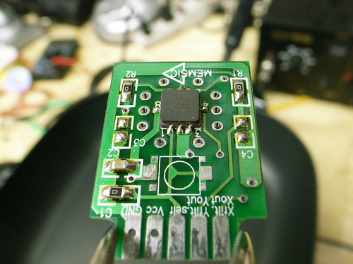
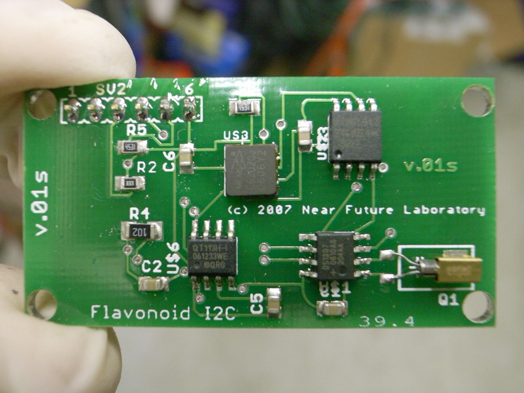
I jump in whole-hog..my first Flavonoid prototype had several I2C devices on a single board and I just sort of “hoped” it all would work..This board has three I2C components on it. A DS1307 real-time clock, some EEPROM device there and a MXC6202J accelerometer. (I stopped using the MEMSIC accelerometers, which work perfectly fine, only they’re designed to use these little heaters inside to do their micro-electronic heat convection technique, and that seemed a little squirrely to me. But, that’s just me.)

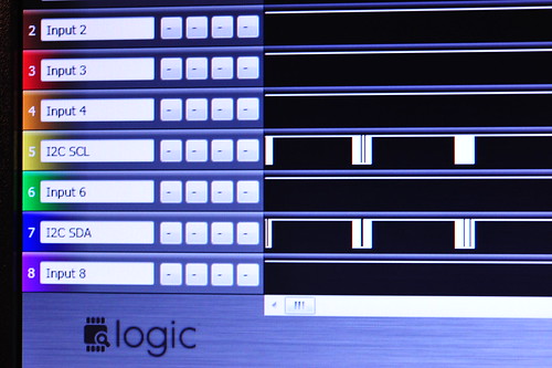
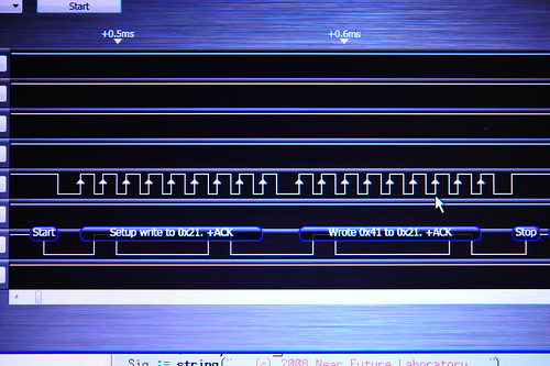
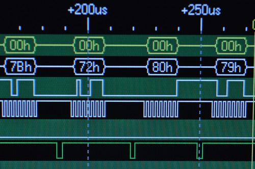
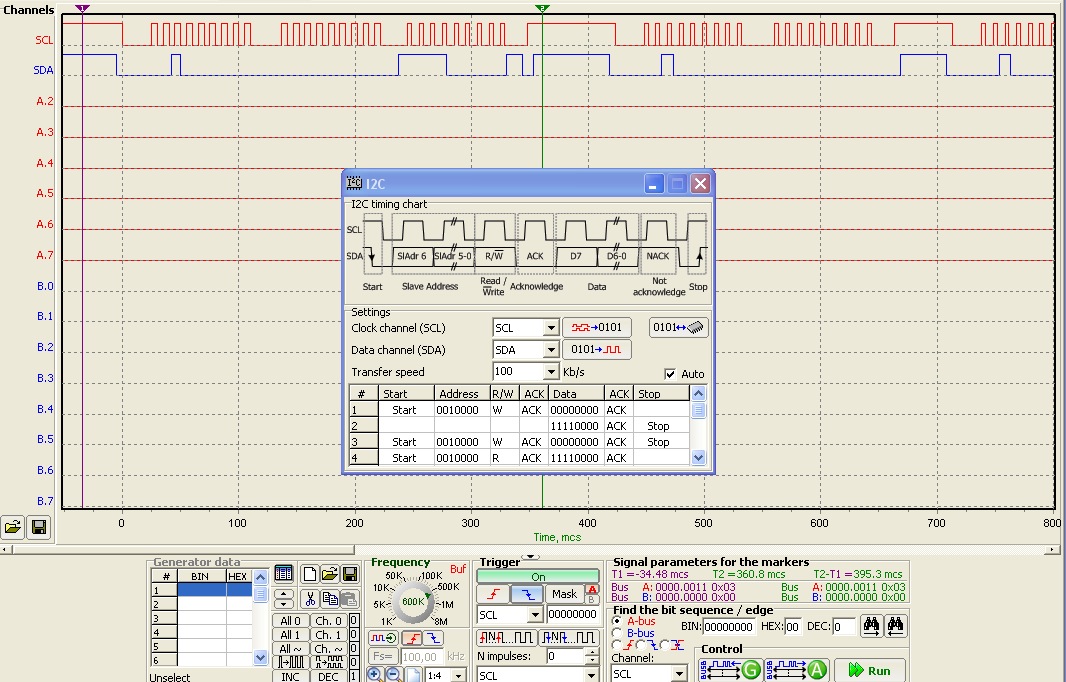
Here’s basically what you see when you put the Logicport software into I2C interpretation mode. I tell it which of its 34 wires are connected to the two I2C lines (SDA and SCL), start up my development hardware and then click the little start acquisition button.

The I2C protocol is fairly straightforward. Essentially it allows one to use two wires to communicate with up to 127 other devices, each with its own address. The protocol is serial-based, so one of those two wires, called SCL, acts as a clock, while the other one, SDA, serializes data down the wire, one bit at a time. The “other devices” down the wire are slave devices that are under the control of a master, maybe some kind of microcontroller. So long as everything on the wire is well-behaved, they’ll listen for data sent to their unique address and handle commands and data appropriately.

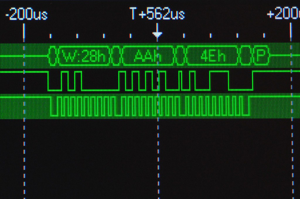
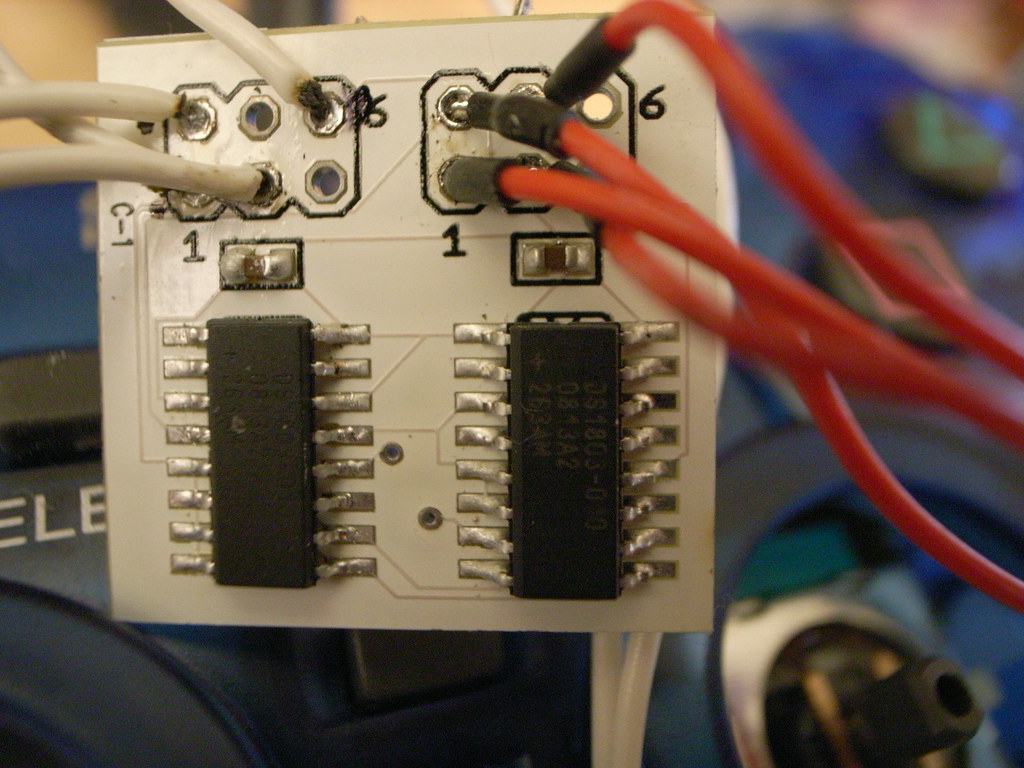
There are safeguards built into the protocol to handle miscommunications, changing over roles between slave and master, multiple masters, etc. The simplest set up — the one I tend to stick with — is one always-and-forever master (a microcontroller, like an Atmega324) and one or several slave devices. There are also contingencies for situations where you want more than one slave of a specific chip. So, for example, here’s a board where I have two DS1803
digital potentiometers. Now, they’re the exact same part number — DS1803 010 (10k digital potentiometer) — and each has factory-burned in the same I2C address. To work around this situation, the part has a three extra pins that you can tie high or low in order to uniquely identify up to 8 of these on one I2C wire.

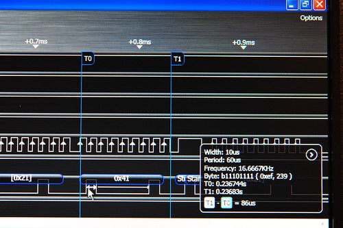
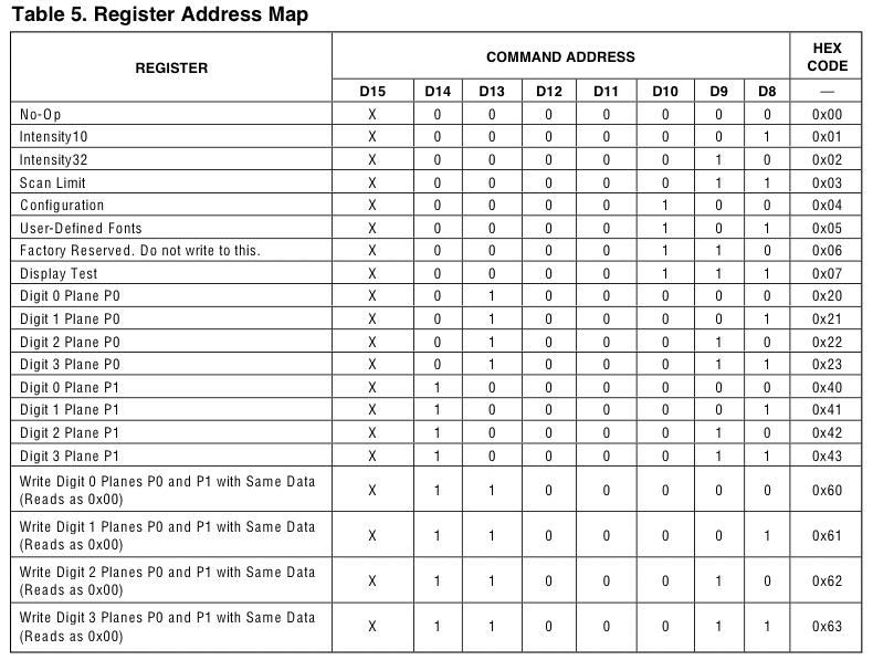
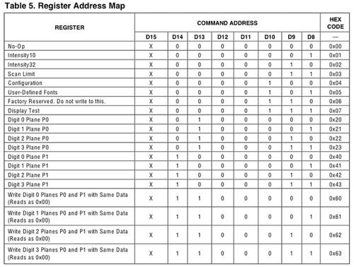
The Logicport and its software begins hunting for the protocol transitions and, hopefully, it’ll find a “start” sequence. In I2C land that’s the master device transitioning SDA from logic high to low while the clock, SCL, remains logic high. So, in that little picture above (click it to blow it up) you can see the mnemonic “S” in the trace indicating the start condition in the top line, where below it the protocol start conditions (SDA high to low, SCL high) are represented. Following that, the I2C protocol expects a sequence of 8 bits representing the slave device address. In this case, I’m testing a MAX6953 which has an address of 0x50h, so all’s good so far. After the end of the slave address is the an “A” which represents the protocol standard “acknowledge” — SDA low while the clock ticks a period. Then there’s this gap followed by another sequence of data which, in this case, is one of several commands I can use to instruct the MAX6953. In this case, the command is represented by a number “0x07h” that is actually an address to a register within the chip.

(It’s a bit confusing, muddling a command code number as a register address — just a bit of memory inside the device — but that can be helpful to think about because many chips using I2C allow you to continue to pump data bytes with the implication that you write the subsequent data to incremental memory addresses, which I describe a bit below.)

According to the MAX6953 specification sheet, allows me to put the display into either “test” mode (all LEDs on) or take it out of “test” mode. By adding an additional parameter to the command, I can control whether it goes into or out of test mode. That parameter is the data that follows the command. In this case, you can see the “acknowledge” and then another sequence of data which happens to be 0x00h — zero. This means that at this point I’m taking the MAX6953 out of test mode and preparing for normal operation. (If I had sent a 0x01h, it would put the MAX6953 into test mode and it would illuminate all of the LEDs in the matrix, useful for testing your wiring and making sure all of the LEDs actually work.)

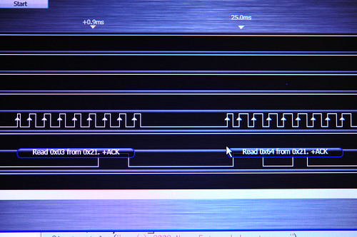
After all that business — the completion of a command and its parameter, in this case — there’s a final sign-off sequence which is the “stop” in which the clock goes high and then the SDA line goes high and, that’s that. Most of the I2C devices I’ve worked with have some features that allow you to continue sending data before the stop with the following bytes of data going to incremental “addresses.” So, for example, in this case I wrote first to address 0x07, which is a register that lives at address “7” inside the chip. Like this:

If I wanted to write to the next register, I could just send another byte of data, rather than having to start all over again with a new command/address, data, etc. This can save clock cycles, when clock cycles matter. In this case, for a few such writes or reads, it’s not a big deal. In other cases, writing to Flash memory, for example, where you’re writing large blocks of data, it can be really useful and tightens things up nicely.

In the PCB below are three I2C components. On the bottom right is a DS1307 I2C Real-Time Clock (you can see the cylindrical crystal used to drive the clock to its right). On the top right is an AT24C1024 1k byte EEPROM chip controlled over I2C. In the kinda top middle is a Memsic I2C two axis accelerometer. By “control” I mean that you can send commands to these to do useful things, depending on what they do. So, for the EEPROM, you can tell it to write data to an address, or read data from an address and send it back across the I2C bus to the master device. The DS1307 can be told to set the day of the month, for example, or say what hour it is.

(A brief design notes about I2C chips. There are lots of them. Often you can find a chip within a family that does the exact same stuff with important variations, like operating voltage differences — 5v versus 3.3v — chip packages — DIP versus surface mount, etc. The useful thing here is that you can swap around as you move from prototyping with an Arduino, for example, which typically wants 5v to run and so the logic rail is 5v for logic high, or a DIP package for easier breadboarding. After all that mess, you can go to smaller, more refined and finished packaging to minimize the footprint.)

Flavonoid v.01s (I2C)

(Flickr)

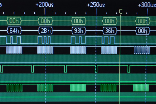
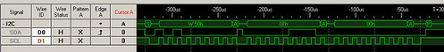
Doing I2C logic analysis with the USB Oscilloscope gives you an image like the one below. It basically shows you the relationship between the clock (SCL) and the serial data line (SDA) and allows you to hunt down gremlins or other problems. How has it saved me? Mostly by saving me time and putting a quick end to real headscratchers.

I have to say, working with I2C has always worked. Eventually. There are two main problems I’ve had.

Number One Problem that I personally have had? Getting the device address wrong, usually by shifting the byte address over in my head by one bit.

Number Two Problem that I personally have had? Forgetting to put pull-up resistors on SDA and SCL. Without pull-ups, the logic levels float too erratically to get a clean and consistent data stream. The logic analyzer will show you stuff, but it won’t make sense and you’ll look at your code and it seems just fine, but the clock and data lines are just floating willy-nilly. So, like..pull-ups. Check that they’re there.

I’ve also tried this USB Oscilloscope thing awhile ago from Hobby Lab. It was relatively cheap — $170 or so, so half as much as the Logicport. (Relative in comparison to the Logicport, and also normal, lab-bench stuff which can run you 100 times as much, easily.) What this sort of device does is offload all the processing and display gymnastics to your PC .

The “box” essentially captures the data, maybe compresses it, and then funnels it across the USB to your PC to figure out how to display it, handling triggering on specific events, etc. The USB Oscilloscope has a digital scope — it comes with a couple of probes like you’d get with a regular scope. But, it also adds a bunch of additional digital channels for sampling up to 16 channels of regular digital data logic analysis, has logic generator feature, so you can pump out sequences of digital data for debugging stuff. I mostly got it for the the logic analysis feature, to help debug I2C and SPI communication when the going go tough.

Here’s a screen shot from a little I2C wrestling using the USB Oscilloscope.

I2C MXC62020J Logic Analysis

There were a few simple analysis features that I believe shouldn’t be too difficult to integrate into the software, but it may turn out that they are not so easy. For example, I want to be able to trigger on certain I2C addresses for example, but I guess that’d be like looking in the future. (It seems to me that you could just buffer a bunch, look for the I2C address following an I2C start and then trigger on this condition. But, I’m not the expert.) There are work-arounds to such things, such as having the Logicport trigger from another unused output pin on the device, and toggling that pin right before the “sequence of interest.” I also find it peculiar that the analysis can continue over and over again — there must be some way of stopping it after a certain number of I2C “frames” have been captured. Must be.

Additional Resources:

Arduino I2C Wire Library

I2C on Wikipedia

Logic Analyzer on Wikipedia

Stuff here at the Near Future Laboratory on I2C

Code to control a MAX6953 from an Arduino, changes the LED matrix to show a number from 0-9 depending on the relative value of a potentiometer connected to Analog In Pin 2 on the Arduino.


#include <Wire.h>

// Using the Wire library (created by Nicholas Zambetti)
// http://wiring.org.co/reference/libraries/Wire/index.html
// On the Arduino board, Analog In 4 is SDA, Analog In 5 is SCL
// These correspond to pin 27 (PC4/ADC4/SDA) and pin 28 (PC5/ADC5/SCL)
on the Atmega8
// The Wire class handles the TWI transactions, abstracting the
nittygritty to make
// prototyping easy.

byte i;
int potPin = 2;
int val = 0;
int ledPin = 13;

void setup()
{
Serial.begin(9600);
Wire.begin(); // join i2c bus (address optional for master)
Wire.beginTransmission(0x50);
Wire.send(0x07); // Display Test
Wire.send(0x00); // Normal Operation
Wire.endTransmission();

Wire.beginTransmission(0x50);
Wire.send(0x01); // Intensity16
Wire.send(0x0F); // Full
Wire.endTransmission();

Wire.beginTransmission(0x50);
Wire.send(0x04); // configuration register
Wire.send(0x01); // disable shutdown mode
Wire.endTransmission();
}

void setCharacter(char c)
{
// if(c >= 0x20 && c <= 0x7F) {
Wire.beginTransmission(0x50);
Wire.send(0x20); // Digit 0 Plane 0
Wire.send(c); // N
Wire.endTransmission();
// }
}

void loop()
{
val = analogRead(potPin);

setCharacter(val/100+‘0’);
delay(300);
}


syntax highlighted by Code2HTML, v. 0.9.1